Toshiba Weds 3D NAND and TSV: Up to 1 TB 3D TLC Chips with 1066 MT/s I/O Incoming
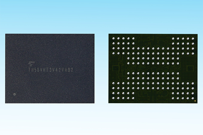
Toshiba on Wednesday introduced its first BiCS 3D TLC NAND flash chips with 512 GB and 1 TB capacities. . The new ICs stack 8 or 16 3D NAND devices using through silicon vias (TSVs) and are currently among the highest capacity non-volatile memory stacks available in the industry. Commercial products powered by the 512 GB and 1 TB packages are expected to hit the market in 2018, with an initial market focus on high-end enterprise SSDs
Stacking NAND devices to build high capacity flash memory ICs has been used for years to maximize the capacities and performance of SSDs and other solid state storage devices. In many cases, NAND makers use wire-bonding technique to stack multiple memory devices, but it makes packages larger and requires a lot of power for reliable operation. However in more recent years, Toshiba has adopted TSV techniques previously used for ASIC and DRAM devices to stack its NAND ICs, which has enabled it to shrink size of its NAND packages and reduce their power consumption.
TSVs are essentially electrodes that penetrate the entire thickness of a silicon die and connect the dies above and below it in the stack. A bus formed by TSVs can operate at a high data transfer rate, consume less power, and take up less space than a bus made using physical wires. Since 3D NAND is based on vertically stacked memory layers and has numerous vertical interconnects, so far Toshiba has not used TSVs to interconnect such devices. To wed TSV and 3D NAND, Toshiba had to develop a special 512 Gb BiCS NAND die featuring appropriate electrical conductors.
It is noteworthy that the company used its 48-layer 2nd generation BiCS architecture instead of the 64-layer 3rd gen BiCS to design the 512 Gb 3D TLC NAND device. The reasons for such design decision are not obvious. On the one hand, 48-layers could minimize the height of the 8-high and 16-high stacks. On the other hand, Toshiba could opt for a lower number of layers because it is using a thicker process technology to build the 3D TLC NAND devices in a bid to improve their endurance (thus, a structure with fewer layers is meant to keep height in check).
Toshiba's 512 GB and 1 TB 3D TLC NAND ICs use a 1066 MT/s Toggle DDR interface, which is one of the advantages that the use of TSVs has enabled. Another advantage enabled by TSVs is a near doubling of Toshiba's data transfer energy efficiency relative to their existing BiCS2-based products that use wire bonding, according to the manufacturer.
| Toshiba's 512 GB and 1 TB 3D TLC NAND Chips | ||
| 512 GB (4096 Gb) | 1 TB (8192 Gb) | |
| Package | NAND Dual x8 BGA-152 | |
| Base Die | 512 Gb 48-Layer BiCS2 3D TLC NAND IC | |
| Number of Stacks | 8 | 16 |
| External Dimensions | Width | 14 mm |
| Depth | 18 mm | |
| Height | 1.35 mm | 1.85 mm |
| Interface | Toggle DDR | |
| Inteface Data Transfer Rate | 1066 MT/s |
The 512 GB and 1 TB 3D TLC NAND chips from Toshiba come in 14i-18 mm packages and use the industry-standard dual x8 BGA-152 interface. The standard pinout is important because the ICs will be used primarily for high capacity SSDs used in servers. In fact, apart from their high density, the 1066 MT/s interface and overall energy efficiency will be the two significant benefits for datacenter-class drives. Further down the line, 512 GB and 1 TB 3D TLC NAND chips will also enable Toshiba and its partners to build 2.5" SSDs with 15 - 30 TB of usable capacity (Samsung uses 512 GB packages to build its flagship PM1633a) and go even higher with 3.5" drives.
Toshiba has already started to ship prototypes of its 512 GB and 1 TB 3D TLC NAND chips for development purposes, and plans to start sampling the 8-high and 16-high flash memory ICs in the second half of 2017. It is hard to make precise predictions about the availability of actual SSDs based on the aforementioned chips, but it is logical to expect them in 2018.
Related Reading: