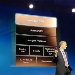
The second keynote of CES comes from NVIDIA, and while it isn't Jensen presenting today, we do get Jeff Fisher, SVP of GeForce, and Ali Kani, VP and GM of NVIDIA's Automotive efforts. There have been rumors about what might be announced today, but follow along to the presentation with us to get all the details!
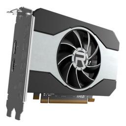
Alongside AMD’s smorgasbord of mobile graphics offerings that were announced during today’s CES 2022 keynote, the company also has some new desktop video cards to speak about for the low-end segment of the market. On January 19 the company will be launching their Radeon RX 6500 XT video card, the long-awaited low-end member of the Radeon RX 6000 series desktop lineup. Based on the new Navi 24 GPU, it will be hitting retail shelves for $199. Meanwhile, joining it a bit later in the year will be the Radeon RX 6400, a second Navi 24 and OEM-only part.
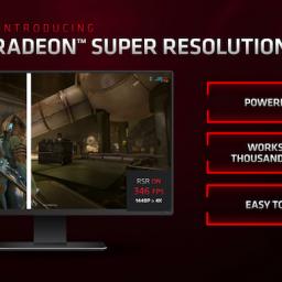
As well as delivering hardware updates for both their desktop and mobile lineups this morning, as part of AMD’s CES 2022 keynote, the company also offered a quick update on their Radeon driver plans for the first quarter of the year. The big takeaway here is that AMD is going to be expanding the accessibility of their FidelityFX Super Resolution image upscaling technology by integrating it into their drivers as a forced override option. Slated to land in a future version of AMD’s driver stack this quarter, the driver-based feature will be promoted as Radeon Super Resolution.As a quick refresher, AMD first released their spatial image upscaling technology, FidelityFX Super Resolution (FSR), back in June. As part of the company’s suite of open source FidelityFX libraries, game developers were free to integrate the image upscaling algorithm into their games by including AMD’s shader program as a step in their image rendering pipeline. The net results of FSR have been mixed from an image quality standpoint, but the shader-based approach is very cheap to execute, and it can be used on a wide range of GPUs (including NVIDIA and Intel parts).AMD has been quick to score a number of developers who have included FSR within their games, but even then, PC gamers have been interested in applying it to additional games. In the last several months this has led to the introduction of utilities like Magpie and Lossless Scaling, which can force various image upscaling techniques on games, including AMD’s FSR. And while forcing FSR in this fashion isn’t ideal from a quality or compatibility standpoint (leading to AMD originally passing on the idea), AMD has since come around on the idea. To that end, AMD will be implementing a form of FSR in their drivers as an override option, which they will be calling Radeon Super Resolution (RSR).As with Magpie and similar utilities, this will be a forced upscaling option that is implemented at the end of the rendering pipeline, rather than the more ideal mid-point. The ramifications of which are that RSR will be upscaling not just the image from the game, but the UI as well; so it will introduce some of the same UI distortion as running a game at a sub-native resolution to begin with.
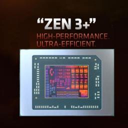
The notebook market is a tough nut to crack with a single solution. People want that mix of high performance at the top, cost effectiveness at the bottom, and throughout there has to be efficiency, utility, and function. On the back of a successful ramp last year, AMD is striking the notebook market hot again in 2022 with the launch of its new Ryzen 6000 Mobile processors. These ‘Rembrandt’ APUs feature AMD’s latest RDNA2 graphics, up to eight Zen3+ cores with enhanced power management features, and it uses TSMC’s N6 manufacturing process for performance and efficiency improvements.
One of the things I look forward to every year is whether the major companies I write about are prepared to showcase their upcoming products in advance – because the year starts with the annual CES trade show, this is the perfect place. A company that’s able to present its 12-month portfolio comes across as confident in its ability to deliver, and it also gets the rest of us salivating at the prospect of next-generation hardware. This time around AMD steps up to the plate to talk about its new V-Cache CPU coming soon, and its new Zen 4 platform coming in the second half of the year.
It's the first week of a new year, which can only mean it's the annual CES trade show! As per usual, the big names have major presentations set up to outline their products for the rest of the year. We're starting bright and early today with AMD first out of the gate, and we're expecting CEO Dr. Lisa Su to present details about the upcoming Ryzen processors as previewed yesterday at the CES awards. Come join us at 7am PT / 10am ET / 15h00 UTC to get all the details.
Ahead of tomorrow’s big CES keynote, AMD is offering a spoiler of sorts for one of their product announcements. As it turns out, one of AMD’s forthcoming products, the Ryzen 6000 Series Mobile processor lineup, is receiving a CES innovation award. And since those awards are being announced this evening, ahead of the show, so too is the Ryzen 6000 Mobile series.While AMD is clearly saving the bulk of the details for tomorrow’s presentation, for this evening they are revealing a few key details. First and foremost, AMD’s latest generation of mobile APUs is getting a significant upgrade in terms of graphics support, with AMD (finally) replacing the Vega GPU architecture with their current-generation RDNA2 GPU architecture. Along with supporting numerous additional graphics features – namely, the DirectX 12 Ultimate feature set – RDNA2 also introduced some significant energy efficiency and computational throughput improvements to AMD’s GPU architecture, which has made AMD’s latest generation of discrete parts among the most competitive in generations.Curiously, no similar mention is made of the underlying CPU architecture. However, since we’re not expecting Zen 4 until later this year, it stands to reason that these new mobile chips are based around the Zen 3 CPU architecture, just like the current Ryzen 5000 chips.AMD Ryzen Mobile APU GenerationsAnandTechCPU ArchGPU ArchMemory TypesYearRyzen 6000 MobileZen 3?RDNA2DDR5 / LPDDR5?2022Ryzen 5000 Mobile (Cezanne)Zen 3VegaDDR4 / LPDDR4X2021Ryzen 4000 Mobile (Renoir)Zen 2VegaDDR4 / LPDDR4X2020AMD’s brief announcement also touts support for newer memory standards, specifically “DDR5 technologies.” All of AMD’s current-generation APUs are currently based around DDR4/LPDDR4, so the move to DDR5 will offer a significant boost to total memory bandwidth, something that should pair very well with the increased iGPU capabilities of the Ryzen 6000 Mobile parts. Notably, LPDDR5 isn’t explicitly mentioned alongside DDR5, but this is clearly a less-than-complete detailing of the chips’ architecture.Finally, the award announcement also confirms that the new Ryzen processors will integrate a Microsoft Pluton-architecture hardware security processor. As well, the chips come with what AMD is calling “AI-audio processing,” which we’ll no doubt hear more about tomorrow.And with that, we’ll have more tomorrow. Join us at 7am PT (15:00 UTC) for our live blog coverage of AMD’s CES 2022 keynote, where we should hear all about the Ryzen 6000 Mobile series and more.
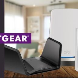
Netgear introduced their first Wi-Fi 6E routers last year with the launch of the Nighthawk RAXE500 and the Orbi RBKE960. The addition of 6 GHz support makes it necessary to include more antennae and add more RF components to the board. As a result, the pricing of these routers tend to be high - the RAXE500 retails for $581 currently (launched with a MSRP of $600), while the basic Orbi RBKE962 (a router and a single satellite) had a launch MSRP of $1100.As part of the 2022 CES launches, Netgear is introducing an affordable Wi-Fi 6E router in the form of the Nighthawk RAXE300. Affordable is a relative term here - the new router has a $400 price point. The cost-down has been achieved by adopting a 8-stream configuration - four in the 5 GHz band, and two each in 6 GHz and 2.4 GHz.Similar to other Nighthawk routers, the RAXE300 also includes the NETGEAR Armor service support, along with a larger number of wired ports compared to mesh systems. A 1Gbps and a 2.5Gbps port are available for WAN connection (the unused one can be repurposed for LAN usage), and link aggregation support is also built in.The USB 3.0 Type-A ports in the previous Nighthawks has now been replaced by a Type-C port. Netgear is also claiming better antenna placement for improved performance.In addition to the RAXE300, the company is also launching the EAX50 6-stream AX5400 extender for $180 later this quarter.Netgear's line of Nighthawk Pro routers has targeted gamers with their Game Booster feature. This allows gamers to restrict connections to geographically close-by servers (based on ping timings and geo-filters), while also providing fine-grained QoS settings to prioritize certain devices / applications over others. Netgear is now adding ad-blocking to the features list.The service is also being rolled out to Orbi owners, with a 30-day free trial, and then billed annually at $50. In recent years, most hardware vendors have shifted to a service model to create a recurrent revenue stream. It is no surprise that Netgear is adding features to and trying to expand their offerings such as Game Booster and ARMOR.Gallery: Netgear Expands Wi-Fi 6E Portfolio with Affordable Nighthawk RAXE300 Router
Netgear Business - the SMB-/SME-focused arm of Netgear - has been delivering mesh Wi-Fi systems to small businesses under the Orbi Pro lineup since 2017. The 802.11ac (Wi-Fi 5) version was followed up by the flagship AX6000 (Wi-Fi 6) Orbi Pro SXK80 models in late 2020. Last year, a cut-down dual-band AX1800 version - the Orbi Pro SXK30 - was introduced at $300. As part of the 2022 CES announcements, the company is introducing the mid-range Orbi Pro model - the SXK50 series.The SXK50 series consists of AX5400 models, with both routers and satellites carrying four wired ports. Netgear is segmenting the models solely based on the hardware, and is keeping business features such as multiple networks, VLAN SSIDs and network isolation / segmentation, etc. consistent across the lineup.The SXK50 (one router and one satellite) is priced at $450 - However, a 5-year Insight Remote Management subscription is included in the price. This tilts the value proposition in its favor despite the absence of the tri-band capabilities seen in the SXK80 series.The Orbi Pro lineup is also getting a new software feature in the form of Insight Business VPN that allows multiple units to form a multi-site VPN connection complete with a common SSID. This allows seamless roaming across both office and home locations for employee devices.In other new hardware announcements, Netgear is also introducing a fanless 2.5Gbps PoE++ switch - the MS108EUP - at $440. This Ultra60 PoE++ Multi-Gigabit Ethernet Plus Switch accommodates a power budget of up to 60W/port (PoE++) for four ports, and 30W/port (PoE+) for the other four, with the total budget not exceeding 230W. PoE++ switches with NBASE-T support are becoming increasingly popular in business circles, thanks to the new 802.11ax access points that have both high power usage and bandwidth capabilities. The recent uptick in PoE-powered business equipment such as IP cameras, speakers, and LED lights has also contributed to this demand.The new MS108EUP switch complements the flagship WAX630 AX6000 access point introduced in mid-2021, enabling full-speed (2.5Gbps) operation with a single uplink cable. The Plus switches come with a simple web-page for configuration, allowing per-port PoE control.Netgear's business arm has been on a roll lately, expanding their portfolio well beyond the switches they had been traditionally known for. Their business mesh systems, in-house access points, and complementary switch models, coupled with a unified cloud-based remote management product (Insight) are presenting SMBs with compelling choices in the market.Gallery: Netgear Introduces Orbi Pro SXK50 AX5400 Mesh System for SMBs
AMD this afternoon has sent out a brief update to the public and investors, offering an update on the status of the ongoing Xilinx acquisition. AMD’s purchase of the FPGA maker, which was previous expected to close by the end of this year, is now expected to close in the first quarter of 2022. Attributing the setback to delays in regulatory approval, AMD believes they’ll be able to finally secure the necessary approval for the $35 billion deal next quarter.As a quick refresher, AMD first announced their intention to buy Xilinx back in October of 2020. The FPGA maker was a lucrative target for AMD, whose sales (and market capitalization) have been growing by leaps and bounds over the last few years. This has brought AMD to the point where they are looking at diversification, as well as covering any gaps in their product lineup that would be holding them back in the server market. As the plan goes, acquiring Xilinx, will allow AMD to offer FPGAs alongside (and potentially integrated with) their current CPU and GPU/accelerator products.The deal was previously expected to close by the end of 2021, and AMD has remained very tight lipped on the matter outside of their initial announcement. None the less, acquiring the necessary regulatory approval is apparently taking AMD longer than planned. According to the company they are not expecting to need to change the deal or alter any of its terms, but they will need another quarter to get the last approvals required to close the deal.“We continue making good progress on the required regulatory approvals to close our transaction. While we had previously expected that we would secure all approvals by the end of 2021, we have not yet completed the process and we now expect the transaction to close in the first quarter of 2022. Our conversations with regulators continue to progress productively, and we expect to secure all required approvals.”
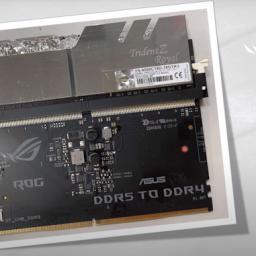
One of the key issues with purchasing a modern Alder Lake system today is the cost of the memory, especially when an enthusiast wants to use DDR5. Due to component shortages, particularly the power management controllers that each DDR5 module needs, costs of DDR5 are quickly rising, with some scalpers looking for $1000+ for basic memory kits. The solution to this has been to recommend that users look to pair Alder Lake with DDR4 memory, which although it isn’t the latest, is the more cost effective scenario. The downside to this solution is that the user has a DDR4-only motherboard, and not the next generation DDR5. That might become a solved issue soon enough, however.In a preview video on YouTube posted today by Bing, who I believe is an ASUS ROG employee, the company has been working on a solution to allow users that buy ASUS Z690 motherboards built on DDR5, to run DDR4 in them. Because Intel limited the platform to either DDR5 or DDR4 per motherboard, there’s no way to run both, until now. In the video, Bing describes the new add-in card they’ve been prototyping.The use case is fairly simple – have a DDR5 board like the ROG Apex, put the carrier card in a memory slot, and place the qualified DDR4 in the top.Obviously, the situation here is more complex than simply using this carrier card. DDR5 and DDR4 are more than simply a notch difference between them – DDR4 is a single 64-bit memory channel per module, while DDR5 is dual 32-bit channel per module. The key issue is that DDR5 does power management per module, where DDR4 relies on power management on the motherboard, so that has to be taken into consideration. Also, adding in a carrier card extends memory traces, which could degrade the quality of the signal.What ASUS does here is use a special BIOS revision to allow the ROG Apex DDR5 to run in DDR4 mode. This means that the traces to the memory slots, although laid out for DDR5 operation, are switched into DDR4 mode. Then, on the carrier card, this takes the 5V power signal and runs it through the equivalent of motherboard power management, and controls the data lines to maintain integrity for signal, latency, power, etc.Bing explains in the video that this is still very much a prototype. It looks like they’re focusing to get it to work on one motherboard with one memory kit first, before optimizing it. Bing states that the carrier card is very tall, and there is room for optimization to make it smaller in the future before ASUS might offer it as a retail product. Also a wider range of validation is likely needed as well.The video goes to show with a single DDR4 module in the carrier card the system running at DDR4-4400 with a Core i5-12600K. To confirm DDR5 still works, the system is shown running dual modules of DDR5-4400, at least to the BIOS screen. If these modules come to market, they are still in early prototypes, and ASUS will likely judge feasibility and demand for them for pricing.Source: YouTube (in Mandarin)
As far as most years ago, 2021 has been an up and down year when it comes to the desktop CPU market. At the beginning of the year, the best CPUs on the market were almost impossible to find, and when they were in stock, it was only above the suggested pricing. Now at the end of the year, processors are plentiful, but the needle has swung in the other direction when it comes to performance. Here’s a rundown of the fun year that 2021 has been.
In a brief news release from Intel this afternoon, the chip firm has announced that it has closed on the first stage of its deal to sell its SSD business to SK hynix. As of today, SK hynix has now formally acquired the bulk of Intel’s NAND and SSD businesses, as well as the company’s NAND fab in Dalian, China. Intel will continue to hold a small stake until 2025, and in the meantime Intel’s former SSD assets have been spun-off into a new SK hynix subsidiary, Solidigm.The Intel-SK hynix deal was first announced in October of 2020, with the two companies inking a deal to transfer over Intel’s NAND and SSD operations over to SK hynix over a several year timeframe. The deal, valued at $9 billion, would see Intel retain all of their Optane/3D XPoint technology and patents, while SK Hynix would receive all of Intel’s NAND-related business, including the Dalian NAND fab and Intel’s SSD business interests.Now, with approval of the deal from all of the necessary regulatory bodies, the two companies have been able to close on the first part of the deal. The “first closing,” as Intel puts it, has transferred the Dalian fab as well as part of Intel’s SSD IP portfolio to SK hynix. Some employees are also being transferred – essentially all those who aren't working for the fab or are involved in R&D. In return, SK hynix has paid Intel the first $7 billion of the deal.The rest of the deal is set to close in three and a half years from now, in or around March of 2025. From now until then, Intel will continue to use the Dalian fab to manufacture NAND wafers. To do so, Intel has held on to some of their NAND-related IP, their R&D employees, and the fab employees. All of those assets will then finally be transferred to SK hynix once the deal fully closes and SK hynix pays Intel the final $2 billion.Finally, SK hynix is taking the Intel assets they’ve acquired thus far and placing them into a new spin-off company, Solidigm. The standalone subsidiary, whose name is apparently a play on “paradigm” and “solid state storage” has set up shop in San Jose, and is being run by former Intel Non-Volatile Memory Solutions Group SVP and GM, Rob Crooke. Solidigm, in turn, has inherited Intel’s current NAND SSD product lineup; this includes Intel’s 660p and 670p client SSDs, as well as their D3/D5/D7 data center SSDs, which are now in the process of becoming Solidigm products.
In a short note published by AMD this afternoon as part of an 8-K filing with the US Securities and Exchange Commission, AMD is disclosing that the company has once again updated its wafer supply agreement with long-time fab partner (and AMD fab spin-off) GlobalFoundries. Under the terms of the latest wafer supply agreement, AMD and GlobalFoundries are now committing to buying and supplying respectively $2.1 billion in wafers for the 2022 through 2025 period, adding an additional year and $500M in wafers to the previous agreement.As a quick refresher, AMD and GlobalFoundries last inked a new wafer supply agreement (WSA) back in May of this year. That agreement further decoupled the two firms, ending any exclusivity agreements between the two and allowing AMD to use any fab for any node as they see fit. None the less, AMD opted to continue buying 12nm/14nm wafers from GlobalFoundries, with the two firms inking a $1.6 billion agreement to buy wafers for the 2022 through 2024 period.Officially classified as the First Amendment to the Amended and Restated Seventh Amendment to the Wafer Supply Agreement, the latest amendment is essentially adding another year’s worth of production to the WSA. The updated amendment now goes through 2025, with AMD raising their 12nm/14nm wafer orders by $500 million to $2.1 billion. AMD and GlobalFoundries are not disclosing the specific per-year wafer supply targets, but the agreement essentially binds GlobalFoundries to supply AMD will a bit over $500M in wafers every year for the next 4 years.Along with yearly spending commitments, the updated agreement also updates the price of said wafers, as well as the pre-payment requirements for 2022/2023. As with the specific number of wafers, AMD isn’t disclosing any further details here.AMD/GlobalFoundries Wafer Share Agreement HistoryAmendment DateDecember 2021May 2021January 2019Total Order Value$2.1B$1.6BN/AStart Date202220222019End Date202520242024GlobalFoundries Exclusivity?NoNoPartial
One of the most agonizing elements of Intel's launch of its latest 12th generation Alder Lake desktop processors is its support of both DDR5 and DDR4 memory. Motherboards are either one or the other, while we wait for DDR5 to take hold in the market. While DDR4 memory isn't new to us, DDR5 memory is, and as a result, we've been reporting on the release of DDR5 since last year. Now that DDR5 is here, albeit difficult to obtain, we know from our Core i9-12900K review that DDR5 performs better at baseline settings when compared to DDR4. To investigate the scalability of DDR5 on Alder Lake, we have used a premium kit of DDR5 memory from G.Skill, the Trident Z5 DDR5-6000. We test the G.Skill Trident Z5 kit from DDR5-4800 to DDR5-6400 at CL36 and DDR5-4800 with as tight timings as we could to see if latency also plays a role in enhancing the performance.
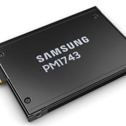
Even though CES 2022 is technically still a couple of weeks away, CES-related announcements are already starting to roll in. Among these are Samsung, who is announcing their first PCIe 5.0 SSD for servers, the PM1743. Based around a new, unnamed PCIe controller, Samsung’s latest server SSD is pairing that with the company’s current (sixth) generation V-NAND. Based on their published specifications, Samsung is touting upwards of 70-90% better performance over their previous-generation drive based on the workload. And tying in with CES in a couple of weeks, the new drive has already been awarded a CES 2022 Innovation Award.At a high level, the PM1743 is the successor to Samsung’s current PM1733 enterprise SSD. Whereas the existing drive is based around a PCIe 4.0 controller and Samsung’s 96L fifth-generation V-NAND, the PM1743 bumps this up to PCIe 5.0 and 128L sixth-generation V-NAND instead. Given the general nature of today’s announcement, the company isn’t offering detailed technical specifications on the drive’s architecture, but between the NAND and controller improvements, they would seem to largely be able to keep up with the additional bandwidth afforded by the move to PCIe 5.0.On paper, the PCie 5.0 x4 link the drive uses can reach bandwidth rates as high as 15.76GB/sec. For the PM1743, in turn, Samsung is claiming peak sequential read rates of 13GB/second, and peak sequential write rates of 6.6GB/sec (presumably to the drive’s SLC cache). This adds up to 86% higher peak read speeds and 89% higher peak write speeds than the PM1733. Or to put that in terms of IOPS, Samsung is claiming that the new drive will be able to hit 2.5M IOPS on random reads, and 250K IOPS on random writes.Samsung Enterprise SSD SpecificationsPM1743
There are many column inches detailing Qualcomm’s design wins and marketing strategy, however to paint it all with a broad brush, it has often boiled down to ‘where can we stick our advanced wireless technology?’. The company has had great success with smartphones, cornering a large chunk of US market and sizeable numbers worldwide, and in the last few years has pivoted to new markets, such as automotive and virtual reality, but also tried to reinvigorate existing markets, such as notebooks and laptops. Since 2017, Qualcomm has wedged a new category into the market, dubbed the ‘Always Connected PC’, offering Windows control with extreme battery life and mobile connectivity. At this year’s Tech Summit, Qualcomm introduced its latest processor, however the real magic might come next year.
TSMC this week announced a new fabrication process that is tailored specifically for high-performance computing (HPC) products. N4X promises to combine transistor density and design rules of TSMC's N5-family nodes with the ability to drive chips at extra high voltages for higher frequencies, which will be particularly useful for server CPUs and SoCs. Interestingly, TSMC's N4X can potentially enable higher frequencies than even the company's next-generation N3 process.One of the problems that is caused by shrinking sizes of transistors is shrinking sizes of their contacts, which means increased contact resistance and consequent problems with power delivery. Various manufacturers use different ways of tackling the contact resistance issue: Intel uses cobalt contacts instead of tungsten contacts, whereas other makers opted to forming contacts using selective tungsten deposition technology. While these methods work perfectly for pretty much all kinds of chips, there are still ways to further improve power delivery for high-performance computing (HPC) designs, which are relatively immodest about the total about of power/voltage being used. This is exactly what TSMC did to its N4X node. But before we proceed to details about the new fabrication process, let us see what advantages TSMC promises with it.TSMC claims that its N4X node can enable up to 15% higher clocks compared to a similar circuit made using N5 as well as an up to 4% higher frequency compared to an IC produced using its N4P node while running at 1.2V. Furthermore – and seemingly more important – N4X can achieve drive voltages beyond 1.2V to get even higher clocks. To put the numbers into context: Apple's M1 family SoCs made at N5 run at 3.20 GHz, but if these SoCs were produced using N4X, then using TSMC's math they could theoretically be pushed to around 3.70 GHz or at an even higher frequency at voltages beyond 1.2V.TSMC does not compare transistor density of N4X to other members of its N5 family, but normally processors and SoCs for HPC applications are not designed using high-density libraries. As for power, drive voltages of over 1.2V will naturally increase power consumption compared to chips produced using other N5-class nodes, but since the node is designed for HPC/datacenter applications, its focus is to provide the highest performance possible with power being a secondary concern. In fact, total power consumption has been increasing on HPC-class GPUs and similar parts for the last couple of generations now, and there is no sign this will stop in the next couple of generations of products, thanks in part to N4X."HPC is now TSMC's fastest-growing business segment and we are proud to introduce N4X, the first in the ‘X’ lineage of our extreme performance semiconductor technologies," said Dr. Kevin Zhang, senior vice president of Business Development at TSMC. "The demands of the HPC segment are unrelenting, and TSMC has not only tailored our ‘X’ semiconductor technologies to unleash ultimate performance but has also combined it with our 3DFabric advanced packaging technologies to offer the best HPC platform."Advertised PPA Improvements of New Process Technologies
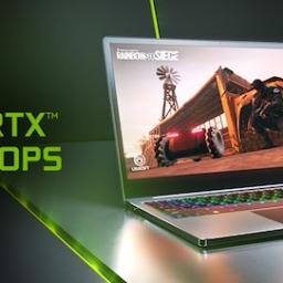
NVIDIA this morning had made an unexpected news drop with the announcement of a trio of new GeForce laptop GPUs. Joining the GeForce family next year will be a new RTX 2000 series configuration, the GeForce RTX 2050, as well as an update to the MX lineup with the addition of the GeForce MX550 and GeForce MX570. The combination of parts effectively provide a refresh to the low-end/entry-level segment of NVIDIA’s laptop product stack, overhauling these products in time for new laptops to be released next year.
Semiconductor makers have drastically increased their capital expenditures (CapEx) this year in response to unprecedented demand for chips that is going to last for years. Now the CEO of Mubadala, the main stockholder of GlobalFoundries, is expecting sales of semiconductors to grow exponentially, toppling a whopping $2 trillion by mid-2030s.“It took 50 years for the semiconductor business to turn into a half a trillion-dollar business," said Khaldoon Al Mubarak, CEO of Mubadala, in an interview with CNBC. "It is going to take probably eight to 10 years to double [by 2030 ~ 2031]. And it is going to double right after that, probably in four to five years.Chipmakers are on track to spend $152 billion on new fabs and production equipment this year, up from $113.1 billion last year. On percentage basis, this is a 34% increase year-over-year, which is the strongest YoY growth since 2017 when cumulative CapEx of semiconductor companies increased by 41% per annum, IC Insights reports.Contract fabs like TSMC, Samsung Foundry, and GlobalFoundries will lead the whole industry in terms of CapEx spending, as they will pour in $53 billion in new fabs and equipment (35% of all semiconductor capital spending in 2021).TSMC, the world's largest foundry, intended to spend between $25 billion and $35 billion on new manufacturing capacities as demand for its services is setting records. Furthermore, the company is preparing to ramp up production of chips using its N3 (3 nm) fabrication technology in 2023 and then N2 (2 nm) node in 2025, which requires buying new tools and building new fabs.IC Insights expects TSMC to be the CapEx champion among all contract makers of chips this year followed by Samsung Foundry. By contrast, SMIC had to cut down its 2021 CapEx to $4.3 billion since it is extremely hard for a company in the U.S. Bureau of Industry and Security's Entity List to procure tools from U.S.-based companies like Applied Materials, KLA, or Lam Research. GlobalFoundries also initiated expansion of production capacities in Germany, Singapore, and the U.S.Meanwhile memory and flash manufacturers are expected to spend $51.9 billion on new fabs and production equipment this year. Since usage of NAND memory is increasing, spending on new flash production capacities is forecasted to reach $27.9 billion, whereas investments in DRAM production will total $24 billion. Interestingly, but CapEx on NAND will grow by 13% year-over-year, whereas expenditures on DRAM will increase by 34% YoY.Microprocessor (MPUs) and microcontroller (MCUs) manufacturers, led by Intel, are on track to raise their CapEx to $23.5 billion this year, up 42% compared to 2020. IC Insights models sales of MPUs and MCUs in 2021 to hit $103.7 billion, up 14% from the previous year, and continue to grow at a compound annual growth rate (CAGR) of 7.1%through 2025, when their sales volume will reach $127.8 billion. Therefore, it is not surprising that companies are gearing up to meet demand for their chips in the coming years.Intel alone expected to spend around $19 billion of CapEx money on expanding its factory network in 2021. While other suppliers of MPUs and MCUs have considerably lower CapEx budgets, they are also boosting their operations and are investing in things like dedicated packaging lines.Most applications that use processors or highly integrated controllers also tend to use different logic devices as well as analog and other components. To that end, suppliers of logic and analog/other devices are also increasing their CapEx spending by 40% and 41% year-over-year respectively as demand for their products is growing rapidly without any signs of slowing down.Related Reading:
One of the key drivers to increase capacity in next generation storage has been to increase the number of bits that can be stored per cell. The easy jump of one to two bits-per-cell gives a straight 100% increase, in exchange for more control needed to read/write the bit but also limits the cell endurance. We’ve seen commercialization of storage up to four bits-per-cell, and talk about five. A Japanese company is now ready to start talking about their new 7 bits-per-cell solution.
Today SK Hynix is announcing the sampling of its next generation DDR5 memory. The headline is the commercialization of a new 24 gigabit die, offering 50% more capacity than the leading 16 gigabit dies currently used on high-capacity DDR5. Along with reportedly reducing power consumption by 25% by using SK Hynix’s latest 1a nm process node and EUV technology, what fascinates me most is that we’re going to get, for the first time in the PC space (to my knowledge), memory modules that are no longer powers of two.For PC-based DDR memory, all the way back from DDR1 and prior, memory modules have been configured as a power of two in terms of storage. Whether that’s 16 MiB to 256 MiB to 2 GiB to 32 GiB, I’m fairly certain that all of the memory modules that I’ve ever handled have been powers of two. The new announcement from SK Hynix showcases that the new 24 gigabit dies will allow the company to build DDR5 modules in capacities of 48 GiB and 96 GiB.To be clear, the DDR5 official specification actually allows for capacities that are not direct powers of two. If we look to other types of memory, powers of two have been thrown out the window for a while, such as in smartphones. However PCs and Servers, as least the traditional ones, have followed the power of two mantra. One of the changes in memory design that is now driving regular modules to non-power of two capacities is that it is getting harder and harder to scale DRAM capacities. The time it takes to figure out the complexity of the technology to get a 2x improvement every time is too long, and memory vendors will start taking those intermediate steps to get product to market.In traditional fashion though, these chips and modules will be earmarked for server use first, for ECC and RDIMM designs. That’s the market that will absorb the early adopter cost of the hardware, and SK Hynix even says that the modules are expected to power high performance servers, particularly in machine learning as well as other HPC situations. One of the quotes on the SK Hynix press release was from Intel’s Data Center Group, so if there is any synergy related to support and deployment, that’s probably the place to start. A server CPU with 8x 64-bit channels and 2 DIMMs per channel gives 16 modules, and 16 x 48 GiB enables 768 GiB capacity.As to when this technology will come to the consumer market, we’re going to have to be mindful of cost and assume that these chips will be used on high-cost hardware. So perhaps 48 GiB UDIMMs will be the first to market, although there’s a small possibility 24 GiB UDIMMs might make an appearance. Suddenly that 128 GiB limit on a modern gaming desktop will grow to 192 GiB.Source: SKHynix Newsroom
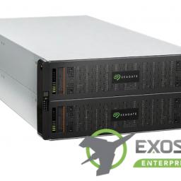
Seagate's Application Platform (AP) series of servers have targeted the market segments requiring tightly coupled storage and compute capabilities. The currently available SKUs - The Exos AP series with HDDs, and Nytro AP series with SSDs - are all based on Intel CPUs. That is changing today with the introduction of the Seagate Exos AP 5U84 based on the AMD EPYC Embedded 7292P processor.The Exos AP 5U84 equipped with the 2nd Gen. AMD EPYC platform enables a high-density building block for private clouds and on-premises equipment, with 84 3.5" HDD bays capable of storing up to 1.344PB (using Exos X16 HDDs) in a 5U form-factor. Capacity can further be expanded with EXOS E SAS expansion units. The platform includes redundancy options and all the other enterprise reliability functions expected in a storage / compute server. Networking with other rack components is enabled by dual port 25GbE controllers. The server processor can be configured for core counts of 8, 12, or 16 depending on required application compute requirements. The EPYC Embedded 7292P processor also include PCIe 4 lanes capable of delivering 200GbE network connectivity, if required.Overall, the core count advantage and per-core power efficiency delivered by EPYC processors make it an ideal addition to Seagate's AP series. Given AMD's steady capturing of the server market, it doesn't come as a surprise to see the AMD EPYC Embedded 7292P getting adopted in the storage market.
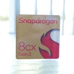
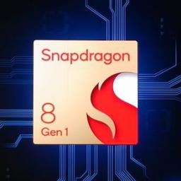
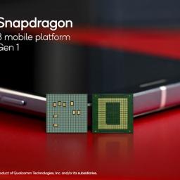
At the recent Qualcomm Snapdragon Tech Summit, the company announced its new flagship smartphone processor, the Snapdragon 8 Gen 1. Replacing the Snapdragon 888, this new chip is set to be in a number of high performance flagship smartphones in 2022. The new chip is Qualcomm’s first to use Arm v9 as well as Samsung’s 4nm process node technology. In advance of devices coming in Q1, we attended a benchmarking session using Qualcomm’s reference design, and had a couple of hours to run tests focused on the new performance core, based on Arm’s X2 core IP.
December is here, and with it comes several technical summits ahead of the holiday break. The most notable of which this week is the annual RISC-V summit, which is being put on by the Linux Foundation and sees the numerous (and ever increasing) parties involved in the open source ISA gather to talk about the latest products and advancements in the RISC-V ecosystem. The summit always tends to feature some new product announcements, and this year is no different, as Imagination Technologies is at the show to provide details on their first RISC-V CPU cores, along with announcing their intentions to develop a full suite of CPU cores over the next few years.The company, currently best known for their PowerVR GPU lineup, has been dipping their toes into the RISC-V ecosystem for the last couple of years with projects like RVfpga. More recently, this past summer the company revealed in an earnings call that they would be designing RISC-V CPU cores, with more details to come. Now at the RISC-V summit they’re providing those details and more, with the formal announcement of their Catapult family of RISC-V cores, as well as outlining a heterogeneous computing-centric roadmap for future development.Starting from the top, the Catapult family is Imagination’s overarching name for a complete family of RISC-V CPU cores, the first of which are launching today. Imagination has (and is) designing multiple microarchitectures in order to cover a broad range of performance/power/area (PPA) needs, and the Catapult family is slated to encompass everything from microcontroller-grade processors to high-performance application processors. All told, Imagination’s plans for the fully fleshed out Catapult family look a lot like Arm’s Cortex family, with Imagination preparing CPU core designs for microcontrollers (Cortex-M), real-time CPUs (Cortex-R), high performance application processors (Cortex-A), and functionally safe CPUs (Cortex-AE). Arm remains the player to beat in this space, so having a similar product structure should help Imagination smooth the transition for any clients that opt to disembark for Catapult.At present, Imagination has finished their first CPU core design, which is a simple, in-order core for 32-bit and 64-bit systems. The in-order Catapult core is being used for microcontrollers as well as real-time CPUs, and according to the company, Catapult microcontrollers are already shipping in silicon as part of automotive products. Meanwhile the real-time core is available to customers as well, though it’s not yet in any shipping silicon.The current in-order core design supports up to 8 cores in a single cluster. The company didn’t quote any performance figures, though bear in mind this is a simple processor meant for microcontrollers and other very low power devices. Meanwhile, the core is available with ECC across both its L1 and TCM caches, as well as support for some of RISC-V’s brand-new extensions, such as the Vector computing extension, and potentially other extensions should customers ask for them.Following the current in-order core, Imagination has essentially three more core designs on their immediate roadmap. For 2022 the company is planning to release an enhanced version of the in-order core as an application processor-grade design, complete with support for “rich” OSes like Linux. And in 2023 that will be followed by another, even higher performing in-order core for the real-time and application processor markets. Finally, the company is also developing a much more complex out-of-order RISC-V core design as well, which is expected in the 2023-2024 timeframe. The out-of-order Catapult would essentially be their first take on delivering a high-performance RISC-V application processor, and like we currently see with high-performance cores the Arm space, has the potential to become the most visible member of the Catapult family.Farther out still are the company’s plans for “next generation heterogeneous compute” designs. These would be CPU designs that go beyond current heterogeneous offerings – namely, just placing CPU, GPU, and NPU blocks within a single SoC – by more deeply combining these technologies. At this point Imagination isn’t saying much more, but they are making it clear that they aren’t just going to stop with a fast CPU core.Overall, these are all clean room designs for Imagination. While the company has long since sold off its Meta and MIPS CPU divisions, it still retains a lot of the engineering talent from those efforts – along with ownership of or access to a large number of patents from the area. So although they aren’t reusing anything directly from earlier designs, they are hoping to leverage their previous experience to build better IP sooner.Of course, CPU cores are just one part of what it will take to succeed in the IP space; besides incumbent Arm, there are also multiple other players in the RISC-V space, such as SiFive, who are all vying for much of the same market. So Imagination needs to both differentiate themselves from the competition, and offer some kind of market edge to customers.To that end, Imagination is going to be heavily promoting the possibilities for heterogenous computing designs with their IP. Compared to some of the other RISC-V CPU core vendors, Imagination already has well-established GPU and NPU IP, so customers looking to put together something more than just a straight CPU will be able to tap into Imagination’s larger library of IP. This does put the company more in direct competition with Arm (who already has all of these things as well), but then that very much seems to be Imagination’s goal here.Otherwise, Imagination believes that their other big advantage in this space is the company’s history and location. As previously mentioned, Imagination holds access to a significant number of patents; so for clients who want to avoid extra patent licensing, they can take advantage of the fact that Imagination’s IP already comes indemnified against those patents. Meanwhile for chip designers who are based outside of the US and are weary of geopolitical issues affecting ongoing access to IP, Imagination is naturally positioned as an alternative there since they aren’t based in the US either – and thus access to their IP can’t be cut off by the US.Wrapping things up, with the launch of their Catapult family of RISC-V CPU IP, imagination is laying out a fairly ambitious plan for the company for the next few years. By leveraging both their previous experience building CPUs as well as their current complementary IP like GPUs and NPUs, Imagination has their sights set on becoming a major player in the RISC-V IP space – and particularly when it comes to heterogeneous compute. Ultimately a lot will need to go right for the company before they can get there, but if they can succeed, then with their diverse collection of IP they would be in a rather unique position among RISC-V vendors.Gallery: Imagination Catapult Slide Deck
In the biggest roadblock yet to NVIDIA’s proposed acquisition of Arm, the United States Federal Trade Commission (FTC) has announced this afternoon that the regulatory body will be suing to block the merger. Citing concerns over the deal “stifling the innovation pipeline for next-generation technologies”, the FTC is moving to scuttle the $40 billion deal in order to protect the interests of the wider marketplace.The deal with current Arm owner SoftBank was first announced in September of 2020, where at the time SoftBank had been shopping Arm around in an effort to either sell or spin-off the technology IP company. And while NVIDIA entered into the deal with bullish optimism about being able to close it without too much trouble, the company has since encountered greater political headwinds than expected due to the broad industry and regulatory discomfort with a single chip maker owning an IP supplier used by hundreds of other chip makers. The FTC, in turn, is the latest and most powerful regulatory body to move to investigate the deal – voting 4-0 to file the suit – following the European Union opening a probe into the merger earlier this fall. TheWhile the full FTC complaint has yet to be released, per a press release put out by the agency earlier today, the crux of the FTC’s concerns revolve around the advantage over other chip makers that NVIDIA would gain from owning Arm, and the potential for misconduct and other unfair acts against competitors that also rely on Arm’s IP. In particular, the FTC states that “Tomorrow’s technologies depend on preserving today’s competitive, cutting-edge chip markets. This proposed deal would distort Arm’s incentives in chip markets and allow the combined firm to unfairly undermine Nvidia’s rivals.”To that end, the FTC’s complaint is primarily focusing on product categories where NVIDIA already sells their own Arm-based hardware. This includes Advanced Driver Assistance Systems (ADAS) for cars, Data Processing Units (DPUs) and SmartNICs, and, of course, Arm-based CPUs for servers. These are all areas where NVIDIA is an active competitor, and as the FTC believes, would provide incentive for NVIDIA to engage in unfair competition.More interesting, perhaps, is the FTC’s final concern about the Arm acquisition: that the deal will give NVIDIA access to “competitively sensitive information of Arm’s licensees”, which NVIDIA could then abuse for their own gain. Since many of Arm’s customers/licensees are directly reliant on Arm’s core designs (as opposed to just licensing the architecture), they are also reliant on Arm to add features and make other alterations that they need for future generations of products. As a result, Arm’s customers regularly share what would be considered sensitive information with the company, which the FTC in turn believes could be abused by NVIDIA to harm rivals, such as by withholding the development of features that these rival-customers need.NVIDIA, in turn, has announced that they will be fighting the FTC lawsuit, stating that “As we move into this next step in the FTC process, we will continue to work to demonstrate that this transaction will benefit the industry and promote competition.”Ultimately, even if NVIDIA is successful in defending the acquisition and defeating the FTC’s lawsuit, today’s announcement means that the Arm acquisition has now been set back by at least several months. NVIDIA’s administrative trial is only scheduled to begin on August 9, 2022, almost half a year after NVIDIA initially expected the deal to close. And at this point, it’s unclear how long a trial would last – and how long it would take to render a verdict.
Western Digital this week said that its energy-assisted magnetic recording (ePMR) and OptiNAND technologies coupled with increased number of platters per hard drive would enable it to build HDDs with an up to 30 TB capacity. To keep advancing capacities from there, the company will need to use heat-assisted magnetic recording (HAMR), it revealed. Meanwhile, noticeably absent was any mention of microwave-assisted magnetic recording (MAMR), the technology that was expected to precede HAMR.Building a 22TB HDD for 2022Last month Western Digital's began shipping its top-of-the-range Ultrastar DC HC560 20TB and WD Gold 20TB hard drives that rely on nine 2.2 TB ePMR platters and feature the company's OptiNAND technology that uses an embedded flash drive (EFD) to increase performance, reliability, and usable capacity of an HDD.To boost capacity of its next-generation hard drives further, Western Digital can either install disks with a higher areal density or increase the number of disks per drive. Both approaches have their challenges (higher areal density might require new heads, whereas an additional platter requires usage of thinner media and mechanical parts), but it looks like the company has a way to put 10 disk into a 3.5-inch HDD."We are able to deliver our 20TB on nine platters, we can add the 10 [disk], and we get another 2.2TB of storage," said David Goeckeler, chief executive of Western Digital (via SeekingAlpha), at the 5 Annual Virtual Wells Fargo TMT Summit Conference.Building a 22TB HDD on a 10-disk platform is a viable way to offer some additional capacity for its customers and stay competitive in 2022. But Western Digital's existing technologies have a considerably more serious potential.Up to 30TBWhen Western Digital introduced its OptiNAND technology earlier this year, it talked about its benefits (which include performance, reliability, and capacity) but did not really quantify them. This week the company finally spilled some beans on the potential of its ePMR technology combined with OptiNAND. As it turns out, it can build 30 TB hard drives using what it already has: ePMR, OptiNAND, and a 10-platter 3.5-inch HDD platform. This will require it to increase areal density of its ePMR disks by about 36%, which is significant."So, we really have that staircase to take you to 30TB and then you get on the HAMR curve and you go for quite a bit longer," said Goeckler. "So, I think it is a really good roadmap for the hard drive industry."MAMR Axed?For years Western Digital envisioned that its MAMR technology as a key enabler of its hard drives with an up to 40TB capacity. In 2019 it introduced its ePMR technology that was considered to be a half-way towards MAMR, but since then the company has barely mentioned MAMR at all.When it announced its OptiNAND technology, Western Digital mentioned MAMR as one of the energy-assisted magnetic recording options it was looking at, but did not reveal any actual plans. At the virtual Wells Fargo summit, Western Digital stressed that HAMR was a key enabler for its future HDDs that have capacity of over 30TB, but did not talk about MAMR at all."HAMR is extremely important, great technology, it is still several years away before it is commercialized, and you can bet your datacenter on it," said Goeckler. "We have heavily invested in HAMR. I think you know we have over 400 patents in HAMR. [If] you are a supplier of hard drives in an industry this big, you are going to [invest] in a number of different technologies that you think is going to fuel your road map. So, we are a big believer in HAMR."If Western Digital can keep expanding capacity of its hard drives with its ePMR technology for a few years before it can roll out its first HAMR-based drives, then it does not need to commercialize its MAMR technology at all since HAMR has considerably better scalability in terms of aerial density.Like every new magnetic recording technology, MAMR and HAMR need to be evaluated by Western Digital's customers before getting to mass production, which takes time. Therefore, it is not in the company's interests to introduce new HDD platforms or new recording technologies too often as this slowdowns adoption of its drives by clients as well as revenue growth.We have reached out to Western Digital to clarify its plans for MAMR, but the company has yet to respond to our request.
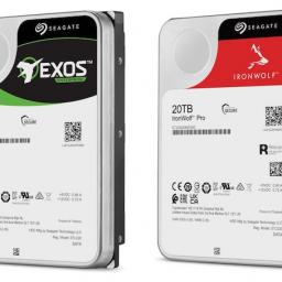
Seagate has updated their flagship capacity options for the retail HDD market with the availability announcement for two new hard drives today - the Exos X20 and IronWolf Pro 20TB. These two models join the recently-released Western Digital WD Gold 20TB and Ultrastar HC560 to round out the 20TB hard drives currently available for retail purchase.The Exos X20 comes with SATA as well as SAS 12Gbps interface options, and includes SED (self-encrypting drive) models while the IronWolf Pro is SATA-only (similar to previous generations). The Exos X20 has a workload rating of 550 TB/yr, while the IronWolf Pro version is rated for 300 TB/yr. A detailed comparative summary of the different specifications of the two new drives and how they stack up against the Western Digital offerings is provided in the table below. Only the SATA options of the Exos X20 and the Ultrastar HC560 are being considered for this purpose. The two model numbers corresponding to these are for the SED and non-SED (standard) options.2021 Retail 20TB HDDs - Comparative SpecificationsSeagate
We're here on Day 2 of the Qualcomm Snapdragon Tech Summit, ready for a keynote on the next generation of Always Connected PCs (ACPCs) and non-Smartphone gaming. We've got new silicon and new handheld devices to talk about.
With 2021 coming to a close, it is time again to look back at the laptop market. Despite bumps from the COVID pandemic, the laptop ecosystem continues to flourish, delivering a bevvy of new products based on new platforms.For 2021, AMD launched their very successful Ryzen 5000 series products (codenamed Cezanne) featuring the latest Zen 3 CPU cores paired with AMD Vega graphics. Intel, still basking in the glow of the Tiger Lake launch in late 2020 continues to feature the 11th generation Core platform that is now over a year old. Based on the Willow Cove cores and featuring a much-improved Intel Xe graphics solution, Intel's solution still provides excellent performance and efficiency for the PC laptop space.The big news of 2021 was Apple ditching x86 processors and beginning the process of moving their products to their in-house designs. While Macs won't be covered in this guide – either you want an Arm-based Mac or you want an x86-based PC – it was still an important milestone in the laptop space and not one to be ignored.
Qualcomm is starting its yearly Snapdragon Tech Summit. We're here to watch CEO Cristiano Amon with the latest updates to the smartphone side of the business.
At this year’s Tech Summit from Hawaii, it’s time again for Qualcomm to unveil and detail the company’s most important launch of the year, and to showcase the newest Snapdragon flagship SoCs that will be powering our upcoming 2022 devices. Today, as the first of a few announcements at the event, Qualcomm is announcing the new Snapdragon 8 Gen 1, the direct follow-up to last year’s Snapdragon 888.
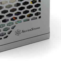
In today’s review we are taking a look at a passively cooled power supply, the SilverStone Nightjar NJ700. Despite the lack of active cooling, the NJ700 can continuously output up to 700 Watts, underscoring its very high efficiency as well as the rest of its impressive electrical specifications. Thanks to it's impeccable design and component selection – courtesy of OEM SeaSonic – the overall performance of the Nightjar NJ700 is world-class, making it more than a match for the even the vast majority of actively cooled 700W PSUs on the market today. Just don't expect one of the best PSUs we've ever reviewed to come cheaply.
After a year of searching for the right place of its new U.S. fab, Samsung this week announced that it would build a fab near Taylor, Texas. The company will invest $17 billion in the new semiconductor fabrication plant and will receive hundreds of millions of dollars in incentives from local and state authorities. Separately, Texas authorities have announced that Texas Instruments intend to spend $30 billion on new fabs in the state, as well.Samsung to Spend $17 Billion on New Texas FabSamsung yet has to disclose all the details about its fab near Taylor, Texas, but for now the company says that the new fab site will occupy an area of over 5 million square meters and will employ 2,000 workers directly and another 7,000 indirectly. To put the number into context, Samsung's fab near Austin, Texas currently employs about 10,000 of workers.Samsung will start construction of the new fab in the first half of 2022 and expects it to be operational in the second half of 2024. It usually takes about a year to construct a building for a semiconductor manufacturing facility and then about a year to install and set up all the necessary equipment.Samsung has not announced which process technologies will be used at its fab near Taylor, Texas, but says it will produce chips for 5G, artificial intelligence (AI), high-performance computing (HPC), and mobile applications, which implies that the fab will gain fairly advanced technologies. In fact, keeping in mind that all of Samsung's nodes thinner than 7 nm rely on extreme ultraviolet (EUV) lithography, it is reasonable to expect the new fab to be EUV capable. As a result, Samsung's customers from the U.S. (such as IBM, Nvidia, and Qualcomm) will be able to produce their chips in the U.S. rather than in South Korea, which might allow their developers to address systems used by the U.S. government."With greater manufacturing capacity, we will be able to better serve the needs of our customers and contribute to the stability of the global semiconductor supply chain," said Kinam Kim, Vice Chairman and CEO, Samsung Electronics Device Solutions Division. "In addition to our partners in Texas, we are grateful to the Biden Administration for creating an environment that supports companies like Samsung as we work to expand leading-edge semiconductor manufacturing in the U.S. We also thank the administration and Congress for their bipartisan support to swiftly enact federal incentives for domestic chip production and innovation."Samsung's new semiconductor production plant will be located 25 kilometers away from the company's fab near Austin, Texas, so the facilities will be able to share infrastructure and resources (such as materials and supplies).Samsung says that it will spend about $6 billion on construction on the building as well as improvements of the local infrastructure. Tools that will be used by the fab will cost another $11 billion. Meanwhile, to build the new plant Samsung will receive hundreds of millions in incentives from the state, the county, and the city, according to media reports. Some of the packages have not been approved yet.Texas Instruments to Invest $30 Billion on New U.S. FabsSamsung is not the only company to build new fabs in Texas. The Governor of Texas recently announced the Texas Instruments was planning to build several new 300-mm fabs near Sherman. In total, TI intends to build as many as four wafer fabrication facilities in the region over coming decades and the cumulative investments are expected to total $30 billion as fabs will be eventually upgraded.Texas Instruments itself yet have to formally announce its investments plans, but the announcement by the governor Greg Abbot indicates that the principal decisions have been made and now TI needs to finalize the details.Sources: Samsung, Austin American-Statesman, Texas.gov
To support the launch of Intel's latest 12th generation 'Alder Lake' processors, Intel has also pulled the trigger on its latest Z690 motherboard chipset. Using a new LGA1700 socket, some of the most significant advancements with Alder Lake and Z690 include PCIe 5.0 support from the processor, as well as a PCIe 4.0 x8 link from the processor to the chipset. In this article, we're taking a closer look at over 30+ different DDR4 enabled motherboards designed to not only use the processing power of Alder Lake but offer users a myriad of high-class and premium features.
We’re nearing the end of the year and the holiday season, and all relevant devices for 2021 have seen their releases, and we’re entering a period of quiet before the industry sees larger refreshes early next year.The biggest shake-up in the last few weeks has been Google’s releases of the Pixel 6 and Pixel 6 Pro. Although the phones are solid and shine in some aspects, their real strength has been in their pricing, which Google offering very compelling value, especially for US readers. This changed up our recommendations at the top-end quite a bit for this month:
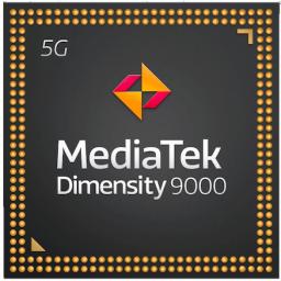
Today, MediaTek is re-entering the flagship SoC space with a bang. The Dimensity 9000 is the first Armv9 SoC, with X2, A710 and A510 cores, large new GPU, massive new ISP, first LPDDR5X, and all in a new TSMC N4 process node.
One of the more curious acquisitions in the last couple of years has been that of Nuvia by Qualcomm. Nuvia was a Silicon Valley start-up founded by the key silicon and design engineers and architects behind both Apple’s and Google’s silicon for the past few years. Qualcomm CEO Cristiano Amon made it crystal clear when Nuvia was acquired that they were going after the high-performance ultraportable laptop market, with both Intel and Apple in the crosshairs.Nuvia came out of stealth in November 2019, with the three main founders having spent almost a year building the company. Gerard Williams III, John Bruno, and Manu Gulati have collectively driven the silicon design of 20+ chips, have combined over 100 patent, and have been in leadership roles across Google, Apple, Arm, Broadcom, and AMD. Nuvia raised a lot of capital, $300M+ over two rounds of funding and angel investors, and the company hired a lot of impressive staff.The goal of Nuvia was to build an Arm-based general purpose server chip that would rock the industry. Imagine something similar to what Graviton 2 and Ampere Altra are today, but with a custom microarchitecture on par (or better) with Apple’s current designs. When Nuvia was still on its own in start-up mode, some were heralding the team and the prospect, calling for the downfall of x86 with Nuvia’s approach. However, Qualcomm swept in and acquired the company in March 2021, and repurposed Nuvia’s efforts towards a laptop processor.It’s been no secret that Qualcomm has been after the laptop and notebook market for some time. Multiple generations of ‘Windows on Snapdragon’ have come to market through Qualcomm’s partners, initially featuring smartphone-class silicon before becoming something more bespoke with the 8cx, 8cx Gen 2, and 7c/7 options in the past couple of years. It has taken several years for Qualcomm to get the silicon and the Windows ecosystem somewhere that makes sense for commercial and consumer use, and with the recent news that Windows 11 on these devices now enabling full x86-64 emulation support, the functional difference between a Qualcomm laptop and an x86 laptop is supposed to be near zero. Qualcomm would argue their proposition is better, allowing for 2 days of use on a single charge, holding charge for weeks, and mobile wireless connectivity with 4G/5G. I’ve tested one of the previous generation S855 Lenovo Yoga devices, and the battery life is insane – but I needed better were functional support (turns out I have an abnormal edge-case work flow…) and more performance. While Qualcomm has been working on the former since my last test, and Nuvia is set to bring the latter.
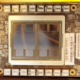
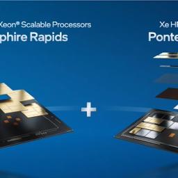
One of the big announcements at AMD’s Data Center event a couple of weeks ago was the announcement of its CDNA2 based compute accelerator, the Instinct MI250X. The MI250X uses two MI200 Graphics Compute Dies on TSMC’s N6 manufacturing node, along with four HBM2E modules per die, using a new ‘2.5D’ packaging design that uses a bridge between the die and the substrate for high performance and low power connectivity. This is the GPU going into Frontier, one of the US Exascale systems due for power on very shortly. At the Supercomputing conference this week, HPE, under the HPE Cray brand, had one of those blades on display, along with a full frontal die shot of the MI250X. Many thanks to Patrick Kennedy from ServeTheHome for sharing these images and giving us permission to republish them.The MI250X chip is a shimmed package in an OAM form factor. OAM stands for OCP Accelerator Module, which was developed by the Open Compute Project (OCP) – an industry standards body for servers and performance computing. And this is the accelerator form factor standard the partners use, especially when you pack a lot of these into a system. Eight of them, to be exact.This is a 1U half-blade, featuring two nodes. Each node is an AMD EPYC ‘Trento’ CPU (that’s a custom IO version of Milan using the Infinity Fabric) paired with four MI250X accelerators. Everything is liquid cooled. AMD said that the MI250X can go up to 560 W per accelerator, so eight of those plus two CPUs could mean this unit requires 5 kilowatts of power and cooling. If this is only a half-blade, then we’re talking some serious compute and power density here.Each node seems relatively self-contained – the CPU on the right here isn’t upside down given the socket rear pin outs aren’t visible, but that’s liquid cooled as well. What looks like four copper heatpipes, two on each side of the CPU, is actually a full 8-channel memory configuration. These servers don’t have power supplies, but they get the power from a unified back-plane in the rack.The back connectors look something like this. Each rack of Frontier nodes will be using HPE’s Slingshot interconnect fabric to scale out across the whole supercomputer.Systems like this are undoubtedly over-engineered for the sake of sustained reliability – that’s why we have as much cooling as you can get, enough power phases for a 560 W accelerator, and even with this image, you can see those base motherboards the OAM connects into are easily 16 layers, if not 20 or 24. For reference, a budget consumer motherboard today might only have four layers, while enthusiast motherboards have 8 or 10, sometimes 12 for HEDT.In the global press briefing, Keynote Chair and Professor world renowned HPC Professor Jack Dongarra, suggested that Frontier is very close to being powered up to be one of the first exascale systems in the US. He didn’t outright say it would beat the Aurora supercomputer (Sapphire Rapids + Ponte Vecchio) to the title of first, as he doesn’t have the same insight into that system, but he sounded hopeful that Frontier would submit a 1+ ExaFLOP score to the TOP500 list in June 2022.Many thanks to Patrick Kennedy and ServeTheHome for permission to share his images.Gallery: AMD’s Instinct MI250X: Ready For Deployment at Supercomputing
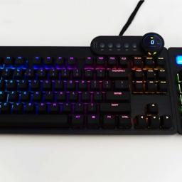
Mountain is a brand that you probably never heard of before in the gaming peripherals industry. The company was founded just a couple of years ago and they currently market only a handful of products. Despite their newcommer status, Mountain went reaching for the top with their first product releases. In today's review, we are taking a look at their mechanical keyboard, the Everest Max, a product designed to rival the best keyboards ever released.
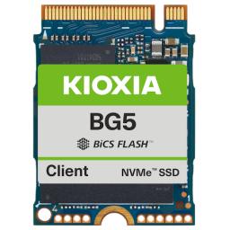
Kioxia this morning is updating their BG series of M.2 2230 SSDs for OEMs with the addition of the new BG5 family of drives. The latest in the company’s lineup of postage stamp-sized SSDs, the BG5 series sees Kioxia reworking both the NAND and the underlying controller to use newer technologies. As a result, the latest iteration of the drive is gaining overall higher performance thanks to the combination of PCIe 4.0 support as well as the switch to Kioxia’s latest BiCS5 NAND. However, in an unexpected twist, the BG series is no longer a single-chip design; instead, the NAND and controller on the BG5 are now separate packages.Long a fixture of pre-built systems, Kioxia’s BG series of SSDs have been a favorite of OEMs for the last several years due to their small size – typically M2. 2230 or smaller – as well as their low cost. In particular, the DRAMless design of the drive keeps the overall component costs down, and it allowed Kioxia to simply stack the NAND dies on top of the controller, giving the SSDs their small footprint. As well, the simple design and tight thermal tolerances of such a stacked design mean that power consumption has been kept quite low, too. The resulting performance of the drives is very much entry-level, and thus rarely noteworthy, but for a drive not much bigger than a postage stamp, it fills a small role.Coming a bit over two years since the BG4 was introduced, the headlining update to BG5 is the addition of PCIe 4.0 support. Whereas BG4 was a PCIe 3.0 x4 drive, BG5 is PCIe 4.0 x4, which at this point gives the drive more bus bandwidth than it could ever possibly hope to use. Truth be told, I was a bit surprised to see that the BG5 went PCIe 4.0 given the limited performance impact on an entry-level drive and the tight power limits, though there are some second-order benefits from PCIe 4.0. In particular, any OEM who ends up only allocating two lanes to the drive (something that happens now and then) will still get the equivalent of PCIe 3.0 x4 speeds out of the drive, which in turn is still high enough to run the drive at almost full performance. This underscores one of the big improvements offered by higher PCIe speeds: for components that don’t need more bandwidth, integrators can instead cut down on the number of lanes.Kioxia BG5 SSD SpecificationsCapacity256 GB512 GB1 TBForm FactorM.2 2230 or M.2 2280InterfacePCIe Gen4 x4, NVMe 1.4NAND Flash112L BiCS5 3D TLCSequential Read3500 MB/sSequential Write2900 MB/sRandom Read500k IOPSRandom Write450k IOPSSpeaking of performance, the BG5 drives are rated for higher throughput than their predecessor. Kioxia’s official press release only offers a single set of figures, so these are almost certainly for the 1TB configuration, but for that drive they are rating it at 2900MB/sec writes and 3500MB/sec reads – the latter just crossing the limits of PCIe 3.0 x4. Random writes and reads are rated at 450K IOPS and 500K IOPS respectively. As always, these figures are against writing to the drive’s SLC cache, so sustained write throughput does eventually taper off.As this is a DRAMless drive, there is no significant on-package caching/buffer layer to talk about. Instead, like its predecessor, Kioxia is relying on Host Memory Buffer (HMB) tech to improve the performance of their drive. HMB isn’t used to cache user data, but instead is used to cache mapping information about the drive’s contents in order to speed up access. Along with the latest generation of this tech, Kioxia has also updated their controller to support NVMe 1.4.Backing the new PCIe 4.0 controller is Kioxia’s BiCS5 generation of TLC NAND, which is a 112L design. BiCS5 has been shipping for a while now, so it’s very much a known quantity, but the time has finally come for it to trickle down into the BG series of drives. BiCS5 was a relatively modest increase in density over BiCS4, so it’s not too surprising here that Kioxia is keeping the largest BG5 configuration at 1TB, which would mean stacking 8 of the 1Tbit dies.But perhaps the biggest change with the BG5 isn’t the specifications of the controller or the NAND on their own, but rather the fact that the two parts are alone to begin with. A staple of the BG5 series design has been the small package enabled by stacking the memory and controller together into a single package. But from Kioxia’s supplied product photo, we can clearly see that the NAND and the controller are separate packages. Kioxia made no mention of this change, so we can only speculate about whether it’s for simplicity in construction (no TSVs to the controller) or maybe the heat put off by a PCIe 4.0 controller. But one way or another, it’s a big change in how the small drive is assembled.As a result of this change, the BGA M.2 1620 form factor – which supplied the single-chip package in a solder-down package – has gone away. Instead, the smallest form factor is now the removable M.2 2230 version. The postage stamp-sized M.2 2230 form factor has long been the staple of the lineup, as it’s what we’ve seen in Microsoft’s Surface products and other thin and light designs over the years. Since the form factor here isn’t changing, the use of multiple packages shouldn’t alter things much for a lot of OEMs. And for OEMs that need physically larger drives for compatibility reasons, Kioxia is also formally offering a 2280 design as well. A simple two-chip solution on such a large PCB is unremarkable, but it would allow the BG5 to be easily inserted into systems that are designed to take (and typically use) 2280 drives.Update 11/22: On the subject of BG5 becoming a two chip solution, Kioxia got back to us with a bit more background information on the change. The change is in part due to gradually increasing power requirements running headlong into the thermal limits of the single chip design. Moving the controller out allows both it and the NAND to be directly cooled, which ultimately allows for better performance at the cost of higher power consumption. More surprising, Kioxia also noted that BGA solutions are falling out of favor with OEMs, whom are swinging back to replaceable/serviceable modules. As a result, Kioxia didn't see a need for a single-chip BGA design for the BG5.As these are OEM drives, no pricing information is available. The drives are currently sampling to Kioxia’s customers, so expect to see them land in commercial products in 2022.
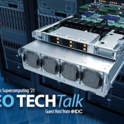
This week we have the annual Supercomputing event where all the major High Performance Computing players are putting their cards on the table when it comes to hardware, installations, and design wins. As part of the event Intel is having a presentation on its hardware offerings, which discloses additional details about the next generation hardware going into the Aurora Exascale supercomputer.
Every once in a while, a startup comes along with something out of left field. In the AI hardware generation, Cerebras holds that title, with their Wafer Scale Engine. The second generation product, built on TSMC 7nm, is a full wafer packed to the brim with cores, memory, and performance. By using patented manufacturing and packaging techniques, a Cerebras CS-2 features a single chip, bigger than your head, with 2.6 trillion transistors. The cost for a CS-2, with appropriate cooling, power, and connectivity, is ‘a few million’ we are told, and Cerebras has customers that include research, oil and gas, pharmaceuticals, and defense – all after the unique proposition that a wafer scale AI engine provides. Today’s news is that Cerebras is still in full startup mode, finishing a Series F funding round.
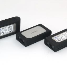
Flash-based portable drives have become popular fast storage options for both content creators and backups-seeking consumers. The advent of high-speed interfaces such as USB 3.2 Gen 2 (10 Gbps) and USB 3.2 Gen 2x2 (20 Gbps) along with Thunderbolt 3 (up to 40 Gbps) have enabled rapid improvements in performance of such portable SSDs over the last few years. While the higher-speed variants have traditionally been premium devices, a push towards lower priced drives was kickstarted by the introduction of native USB flash drive (UFD) controllers. Today, we are taking a look at the performance and value proposition of the complete Kingston XS2000 portable SSD lineup based on the Silicon Motion SM2320 controller.
To support the launch of Intel's latest 12th generation 'Alder Lake' processors, Intel has also pulled the trigger on its latest Z690 motherboard chipset. Using a new LGA1700 socket, some of the most significant advancements with Alder Lake and Z690 include PCIe 5.0 support from the processor, as well as a PCIe 4.0 x8 link from the processor to the chipset. In this article, we're taking a closer look at over 50+ different DDR5 enabled motherboards designed to not only use the processing power of Alder Lake but offer users a myriad of high-class and premium features.
Alongside a slew of software-related announcements this morning from NVIDIA as part of their fall GTC, the company has also quietly announced a new server GPU product for the accelerator market: the NVIDIA A2. The new low-end member of the Ampere-based A-series accelerator family is designed for entry-level inference tasks, and thanks to its relatively small size and low power consumption, is also being aimed at edge computing scenarios as well.Along with serving as the low-end entry point into NVIDIA’s GPU accelerator product stack, the A2 seems intended to largely replace what was the last remaining member of NVIDIA’s previous generation cards, the T4. Though a bit of a higher-end card, the T4 was designed for many of the same inference workloads, and came in the same HHHL single-slot form factor. So the release of the A2 finishes the Ampere-ficiation of NVIDIA accelerator lineup, giving NVIDIA’s server customers a fresh entry-level card.NVIDIA ML Accelerator Specification ComparisonA100A30A2FP32 CUDA Cores691235841280Tensor Cores43222440Boost Clock1.41GHz1.44GHz1.77GHzMemory Clock3.2Gbps HBM2e2.4Gbps HBM212.5Gbps GDDR6Memory Bus Width5120-bit3072-bit128-bitMemory Bandwidth2.0TB/sec933GB/sec200GB/secVRAM80GB24GB16GBSingle Precision19.5 TFLOPS10.3 TFLOPS4.5 TFLOPSDouble Precision9.7 TFLOPS5.2 TFLOPS0.14 TFLOPSINT8 Tensor624 TOPS330 TOPS36 TOPSFP16 Tensor312 TFLOPS165 TFLOPS18 TFLOPSTF32 Tensor156 TFLOPS82 TFLOPS9 TFLOPSInterconnectNVLink 3
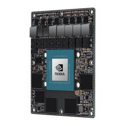
Today as part of NVIDIA’s fall GTC event, the company has announced that the Jetson embedded system kits will be getting a refresh with NVIDIA’s forthcoming Orin SoC. Due early next year, Orin is slated to become NVIDIA’s flagship SoC for automotive and edge computing applications. And, has become customary for NVIDIA, they are also going to be making Orin available to non-automotive customers through their Jetson embedded computing program, which makes the SoC available on a self-contained modular package.Always a bit of a side project for NVIDIA, the Jetson single-board computers have none the less become an important tool for NVIDIA, serving as both an entry-point for helping bootstrap developers into the NVIDIA ecosystem, and as a embedded computing product in and of itself. Jetson boards are sold as complete single-board systems with an SoC, memory, storage, and the necessary I/O in pin form, allowing them to serve as commercial off the shelf (COTS) systems for use in finished products. Jetson modules are also used as the basis of NVIDIA’s Jetson developer kits, which throw in a breakout board, power supply, and other bits needed to fully interact with Jetson modules.NVIDIA Jetson Module SpecificationsAGX OrinAGX XavierJetson NanoCPU12x Cortex-A78AE