HBM3: Cheaper, up to 64GB on-package, and terabytes-per-second bandwidth

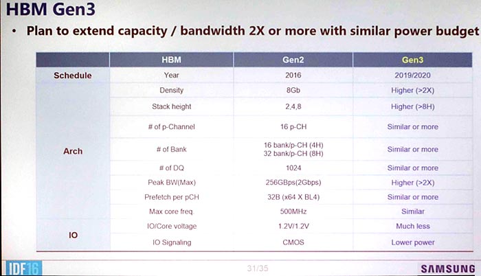
Despite first- and second-generation High Bandwidth Memory having made few appearances in shipping products, Samsung and Hynix are already working on a followup: HBM3. Teased at the Hot Chips symposium in Cupertino, Calfornia, HBM3 will offer improved density, bandwidth, and power efficiency. Perhaps most importantly though, given the high cost of HBM1 and HBM2, HBM3 will be cheaper to produce.
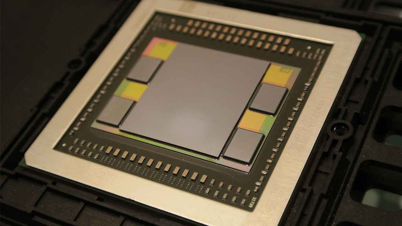
With conventional memory setups, RAM chips are placed next to each other on a circuit board, usually as close as possible to the logic device (CPU or GPU) that needs access to the RAM. HBM, however, stacks a bunch of RAM dies (dice?) on top of each other, connecting them directly with through-silicon vias (TSVs). These stacks of RAM are then placed on the logic chip package, which reduces the surface area of the device (AMD's Fury Nano is a prime example), and potentially provides a massive boost in bandwidth.
The tradeoff, though, as with most fancy packaging techniques, has been price and capacity. HBM1, as used in AMD's Fury graphics cards, was limited to 4GB stacks. HBM2, as used in Nvidia's workstation-only P100 graphics card, features higher density stacks up up to 16GB, but is prohibitively expensive for consumer cards.
Read 6 remaining paragraphs | Comments