 |
by Ganesh T S on (#65KCG)
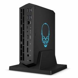
Intel is officially taking the wraps off the first member of their Raptor Lake-based NUC13 family today. The NUC13 Extreme (like the three previous Extreme NUCs) caters to the gamers and content creators requiring leading edge performance and high-end discrete GPU support. Unlike the mainstream NUCs which have been consistently maintaining an ultra-compact form-factor profile, the Extreme family has slowly grown in size to accommodate flagship CPUs and discrete GPUs. These systems integrate a motherboard in a PCIe add-in card form factor (the Compute Element) and a baseboard that provides additional functionality with PCIe slots and other I/O features. As a refresher, Intel created the NUC Extreme category with the introduction of the Ghost Canyon NUC family in 2019. This was followed by the Tiger Lake-based Beast Canyon NUC in 2021 and the Alder Lake-based Dragon Canyon NUC earlier this year. The latest member of this family is today's introduction - the Raptor Canyon NUC based on the Shrike Bay Compute Element.The NUC Extreme family has grown in physical footprint with each generation, and the NUC13 Extreme is Intel's biggest one yet. Coming in at 317mm x 129mm x 337mm (13.7L), this is more of a traditional tower desktop than the NUCs that the market has grown accustomed to. However, this size has allowed Intel to integrate flagship components. The Shrike Bay Compute Element supports socketed LGA 1700 processors with a PL1 of 150W and PL2 of 250W (tau of 28s). The vertical centering of the baseboard within the case enables plenty of isolation between the Compute Element on the top and the discrete GPU on the bottom. Triple-slot dGPUs up to 12.5" in length are supported.The NUC13 Extreme Kit comes in three flavors, while the Shrike Bay Compute Element itself has six variations. These allow system integrators and OEMs to offer a wide variety of systems targeting different market segments. The table below summarizes the key differences between the three NUC13 Extreme kits.Intel NUC13 Extreme Kits (Raptor Canyon)ModelNUC13RNGi9NUC13RNGi7NUC13RNGi5CPUIntel Core i9-13900K
|
| Link | https://anandtech.com/ |
| Feed | https://anandtech.com/rss/ |
| Updated | 2024-04-26 07:15 |
 |
by Ganesh T S on (#38WE7)
Data storage requirements have kept increasing over the last several years. While SSDs have taken over the role of the primary drive in most computing systems, hard drives continue to be the storage media of choice in areas dealing with large amount of relatively cold data. Hard drives are also suitable for workloads that are largely sequential and not performance sensitive. The $/GB metric for SSDs (particularly with QLC in the picture) is showing a downward trend, but it is still not low enough to match HDDs in that market segment.Since the release of the last HDD guide, the availability of Western Digital's OptiNAND-equipped 22TB drives has improved, and Toshiba's new Pro lines for their X300 and N300 lineups have started coming down in price. The high-capacity last-generation (20TB) models have become a lot more affordable - selling prices are running around 15 - 20% lower than launch MSRPs. These make for an interesting update to our list of recommended hard drives for NAS and desktop usage.
|
 |
by Ryan Smith on (#65EGX)
With AMD’s first-wave of Zen 4 CPUs now in the books with the Ryzen 7000 series, the consumer arm of AMD is now shifting its attention over to its graphics business. In a presentation that ended moments ago dubbed “together we advance_gaming”, Dr. Lisa Su and other AMD leaders laid out the future of AMD’s graphics products. And that future is the RDNA 3 architecture, which will be the basis of the new Radeon RX 7900 XTX and Radeon RX 7900 XT video cards.The two cards, set to be released on December 13, will be the first products released using the RDNA 3 architecture. According to AMD, the new flagship 7900 XTX will deliver up to 70% more performance at 4K than their previous flagship, the 6950 XT. This performance boost comes curtesy of several architectural improvements in RDNA that cumulatively offer 54% higher performance per watt than RDNA 2, as well as higher clockspeeds courtesy of TSMC’s 5nm (and 6nm) processes, and higher overall power consumption.The full-fledged RX 7900 XTX will be hitting the streets at $999. Meanwhile the second-tier RX 7900 XT will run for $899.
|
 |
by Ryan Smith & Gavin Bonshor on (#65E3P)
Following hot on the heels of AMD’s major CPU launch of the year – the Zen 4 architecture and Ryzen 7000 family – today AMD will be giving their GPU architecture its moment in the sun with their gaming-centric “together we advance_gaming” event. Today’s event will be all about AMD’s next-generation Radeon GPU architecture, RDNA 3, which among other things, promises a 50% improvement in performance-per-watt over the previous-generation RDNA 2 (Radeon RX 6000 series) parts.Notably, unlike AMD’s CPU event back in August, AMD has held their (video) cards closer to their proverbial chest for this event. We know that it’s all about the RDNA 3 architecture, but AMD is being quieter about product information and details. For example, any “Radeon RX 7000 series” branding is completely absent from all of AMD’s official communiques. So while the Radeon RX 7000 series is still the branding we’re expecting to see, AMD is leaving themselves a noticeable amount of room to throw some curveballs here.In any case, AMD has offered a few high-level details on the RDNA 3 architecture throughout the year. The biggest items disclosed thus far are that AMD is targeting another 50% increase in performance-per-watt, and that these new GPUs (Navi 3x) will be made on a 5nm process (undoubtedly TSMC’s). Past that, AMD hasn’t given any guidance on what to expect for performance.One interesting aspect, however, is that AMD has confirmed that they will be employing chiplets with this generation of products. To what extent, and whether that’s on all parts or just some, remains to be seen. But chiplets are in some respects the holy grail of GPU construction, because they give GPU designers options for scaling up GPUs past today’s die size (reticle) and yield limits. That said, it’s also a holy grail because the immense amount of data that must be passed between different parts of a GPU (on the order of terabytes per second) is very hard to do – and very necessary to do if you want a multi-chip GPU to be able to present itself as a single device.We’re also apparently in store for some more significant upgrades to AMD’s overall GPU architecture. Though what exactly a “rearchitected compute unit” and “optimized graphics pipeline” fully entail remains to be seen.The answers to all that, and more, are coming up here in a few hours. So be sure to join us today, November 3, at 1pm Pacific (20:00 UTC) for our full live blog coverage of AMD’s latest GPU announcements. We can’t wait!
|
 |
by Gavin Bonshor on (#38T05)
It has been a busy couple of months for both Intel and AMD, as well as their partner motherboard manufacturers. The release of AMD's latest Ryzen 7000 series processors back in September marked the start of a new era for AMD and its AM5 platform – although AM4 isn't quite dead yet.With the launch of Ryzen 7000 and AM5 comes support for DDR5 memory, which provides benefits to performance and gets AMD setup to use what is becoming the current generation of memory for the industry. But unlike Intel's 13th and 12th Gen Core series processors, AMD dropped any support for DDR4 memory, opting to fully focus on next-generation memory and the long-term prospects of the platform. This has meant that users looking to build a Ryzen 7000 system will not be able to recycle any DDR4 memory they already have, and instead will need to buy DDR5 to work with AM5.Regardless of whether you're looking to build a new system or upgrade an older one, AMD has a wide range of processors to cover all use cases. Its AM4 platform has been a highly successful one for AMD, giving us the likes of Ryzen 1000 (Zen), Ryzen 2000 (Zen+), and even Ryzen 3000 (Zen 2) and Ryzen 5000 (Zen 3). With the launch of Ryzen 7000 processors to the market, it has delivered better performance in applications, content creation, rendering, and gaming than it ever has before. So while no longer the new and shiny thing from AMD, AM4 is still a viable platform and will remain so for well into 2023.Given that AMD is in the midst of this transition, for our latest buyers guide we have opted to split our selections between AM4 and AM5. Despite Ryzen 7000 dominating performance charts, there is still quality and value to be found from AM4, especially at the lower end. So without further adu, here are our picks for AMD motherboards for the 2022 holiday period.
|
 |
by E. Fylladitakis on (#6572R)
In today's review, we are taking a look at the ValuePro VP1600ELCD, a popular low-cost UPS from CyberPower, the renowned US-based power systems manufacturer. As the name suggests, it is a product developed with value in mind, in an effort to entice home users and small business owners. Truly, features such as built-in AVR and completely silent operation are very enticing at this price range from a renowned brand name. As with all things that are too good to be true though, there are tradeoffs.
|
 |
by Ryan Smith on (#656N7)
While always an interesting topic by default, corporate earnings reports in the tech industry have become especially important in the last few months, as the industry prepares to weather what’s expected to be the biggest downturn in demand in the last several years. Intel’s brutal Q2’22 report, which found the company losing money on a GAAP basis for the first time in 5 years, seems to have been a herald of things to come for the largest industry, with AMD and other companies since issuing earnings warnings ahead of their own Q3 reports. So as the first major tech company to publish their complete Q3’22 earnings report, Intel is once again likely to be a barometer of the tech industry’s performance over the past three months.For the third quarter of 2022, Intel reported $15.3B in revenue, a $3.9B decline versus the year-ago quarter. Compared to Intel’s harsh Q2 report, the company has returned to profitability, booking a cool billion dollars in net income, though this is still well below their historical norms. In fact, the company is still operating at a (GAAP) loss, booking an operating income of -$175M. For Q3 at least, it would appear that it’s Intel’s tax situation that’s pushing them into the black, with the company recording a $1.2B tax benefit.
|
 |
by Anton Shilov on (#656D1)
Currently the majority of high-end processors are monolithic, but design methodologies are slowly but surely shifting to multi-chiplet modules as leading-edge fabrication technologies get more expensive to use. In the coming years multi-chiplet system-in-packages (SiPs) are expected to become much more widespread, and advanced 2.5D and 3D chip packaging technologies will gain importance. To accelerate and simplify development of 3D designs, TSMC this week established its 3DFabric Alliance.While multi-chiplet SiPs promise to simplify development and verification of highly complex designs, they require brand-new development methodologies as 3D packages bring a number of new challenges. This includes new design flows required for 3D integration, new methods of power delivery, new packaging technologies, and new testing techniques. To make the best use of the benefits of TSMC's 2.5D and 3D packaging technologies (InFO, CoWoS, and SoIC), the chip development industry needs the whole ecosystem to work in concert on chiplet packaging – and this is what 3DFabric Alliance is designed to do.“3D silicon stacking and advanced packaging technologies open the door to a new era of chip-level and system-level innovation, and also require extensive ecosystem collaboration to help designers navigate the best path through the myriad options and approaches available to them,” said Dr. L.C. Lu, TSMC fellow and vice president of design and technology platform.TSMC's 3DFabric Alliance brings together developers of electronic design automation (EDA) tools, intellectual property providers, contract chip designers, memory manufacturers, advanced substrate producers, semiconductor assembly and test companies, and the groups making the equipment used for testing and verification. The alliance currently has 19 members, but over time it is expected to expand as new members join the group.As the leader of the Alliance, TSMC will set certain ground rules and standards. Meanwhile members of 3DFabric Alliance will co-define and co-develop some of the specifications for TSMC's 3DFabric technologies, will gain early access to TSMC's 3DFabric roadmap and specs to align their plans with the foundry's plans as well as those of other members of the alliance, and will be able to design and optimize solutions that are compatible with the new packaging methods.Ultimately, TSMC wants to ensure that members of 3DFabric Alliance will offer its clients compatible and interoperable solutions that will enable quick development and verification of multi-chiplet SiPs that use 2.5D and 3D packaging.For example, to unify the design ecosystem with qualified EDA tools and flows, TSMC has developed its 3Dblox standard. 3Dblox covers various aspects of building multi-chiplet devices featuring 2.5D and 3D packaging methodologies (such as chiplet and interface definitions), including physical implementation, power consumption, heat dissipation, electro-migration IR drop (EMIR), and timing/physical verification.“Through the collective leadership of TSMC and our ecosystem partners, our 3DFabric Alliance offers customers an easy and flexible way to unlocking the power of 3D IC in their designs, and we can’t wait to see the innovations they can create with our 3DFabric technologies,” added Lu.Ultimately, TSMC envisions that the alliance will greatly simplify and streamline the process for developing more advanced chips, especially for small and mid-size companies that rely more heavily on outside IP/designs. For example, if a company wants to develop a SiP consisting of logic chiplets stacked together and connected to an HBM3-based memory subsystem, EDA software from Ansys Cadence, Synopsys, and Siemens will allow it to design compatible chiplets, IP providers will sell those blocks the designer does not already have, TSMC will produce silicon, memory producers will offer compatible HBM3 KGSDs (known good stack dies), and then Ase Technology will assemble everything together. Meanwhile companies that do not have their own engineers will be able to order the design of the whole SiP (or individual chiplets) through Alchip or GUC, and then update their product over time if needed without needing to redesign everything, as the SiP will be built in accordance with 3DFabric and 3Dblox standards.3Dblox is currently supported by four major EDA developers. Eventually it will be supported by all members of the members if the alliance where needed.While large companies like AMD and Nvidia tend to develop their own IP, interconnection, and packaging technologies, multi-chiplet SiPs promise to make the development of complex, chiplet-style processors accessible to smaller companies. For them, standard third-party IP, fast time-to-market, and proper integration are key to success, so 3DFabric Alliance and what it brings will be vital for them.Source: TSMC
|
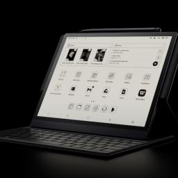 |
by Ganesh T S on (#655J7)
The e-Paper market has enjoyed steady growth over the last decade, starting with the introduction of the Amazon Kindle back in 2007. While there are many vendors attempting to make a mark in the technology required in this space, E-Ink's offerings have ruled the roost.The most popular category of products using E-Ink's technology has undoubtedly been eBook readers. Recently, digital notebooks and notepads have also emerged as a significant driver in E-Ink's expansion. These products take the regular e-reader and add support for an electronic pen / stylus. These products were initially quite expensive and targeted business professionals dealing with huge amounts of paperwork and requiring note-taking support (such as lawyers). The Sony DPT lineup (review) became one of the leading products in this category. As the market expanded, vendors such as reMarkable and ONYX also started putting out compelling products - expanding the target market to creative professionals and students as well. This category became truly mass-market a few months back with the introduction of Amazon's Kindle Scribe (and slated to start shipping in time for the holiday season).ONYX has been serving the e-reader market since 2006. They have an extensive lineup of e-readers (both grayscale and color), e-Paper tablets with note-taking support, and even E-Ink monitors. Today, the company is launching a new category - ePaper Tablet PCs. The first product in this lineup is the ONYX BOOX Tab Ultra - a 10.3" unit complete with a 16MP rear-facing camera. A first for E-Ink devices, ONYX envisages the camera being used to OCR documents in the field without the need for an external device as an intermediary. The device targets professional use-cases. It must be noted that ONYX already carries the BOOX Note Air 2 Plus that carries most of the same features, but geared towards the home / casual consumer.The ONYX BOOX Tab Ultra is the first e-reader model from ONYX to utilize the company's proprietary fast refresh algorithm implemented using a separate hardware module on the board. The company has been using this on its Mira lineup of E-Ink monitors, and its use in the e-reader is supposed to improve user experience with web content. Scrolling, in particular, has been a weak point of E-Ink tablets due to the low refresh rate. The actual improvements delivered by the ONYX 'BSR' (BOOX Super Refresh) algorithm in this aspect needs hands-on evaluation for further analysis. The system supports four different modes for different tasks - reading books doesn't require fast refreshing and can utilize the 'HD Mode', while typing requires a 'Balance Mode'. A 'Fast Mode' is available for web browsing, and an 'Ultrafast Mode' for generic Android applications.The BOOX Tab Ultra utilizes a Qualcomm Snapdragon 662 SoC (4x Kyro Gold (A73-class) @ 2GHz + 4x Kyro Silver (A53-class) @ 1.8 GHz, along with an Adreon 610 GPU), and comes with a specialized version of Android 11 (including Play Store support). The unit is equipped with a 6300 mAh battery, 4GB of LPDDR4x DRAM, and 128GB of eMMC flash storage. The USB-C port in the system also supports OTG functionality, and a micro-SDXC card slot. A keyboard case with a magnetic holder for the Tab Ultra is also available.ONYX has a reputation for long support cycles, and provides regular firmware updates to augment the functionality of its ePaper tablets. Recent firmware updates have brought a more tablet-like experience in the user interface - a home screen with apps along with a favorites dock at the bottom. ONYX claims that the use of Android in its tablets (compared to custom OSes in other products such as the Kindle Scribe and reMarkable tablets) enables its customers to take advantage of the host of personal knowledge management apps available for note taking and data collection. Another recently added functionality relates to the association of different pages in different documents using easily-created tags.The ONYX BOOX Tab Ultra is available for pre-order today and comes with a $600 price tag. The company is also simultaneously releasing the Nova Air 2 7.8" e-Paper tablet with stylus support at $400 and the Leaf 2 7" e-reader at $200. ONYX has typically not hesitated in trying out innovative ideas on the e-Paper front (they were one of the first vendors to bring out color e-readers), and equipping an e-reader / digital notebook with a rear camera is yet another interesting play from the company. The new products expand ONYX's target market and build upon its position as one of the leading E-Ink product vendors in the market in the face of rising competition.
|
|
by Ryan Smith on (#64YE5)
Following on the heels of AMD’s CPU-centric event back in August, AMD today has sent out a press release announcing that they will be holding a similar event in November for their Radeon consumer graphics business. Dubbed “together we advance_gaming”, the presentation is slated to be all about AMD Radeon, with a focus on the upcoming RDNA 3 graphics architecture and all the performance and power efficiency benefits it will bring. The event is set to kick off on November 3 at 1pm PT (20:00 UTC), with undisclosed AMD executives presenting details.Like the Ryzen event in August, next month’s Radeon event appears to be AMD gearing up for the launch of its next generation of consumer products – this time on the GPU side of matters. Back at the start of the summer, AMD confirmed that RDNA 3 architecture products were scheduled to arrive this year, so we have been eagerly awaiting the arrival of AMD’s next generation of video cards.Though unlike AMD’s CPU efforts, the company has been far more mum about its next-gen GPU efforts. So details in advance on what will presumably be the Radeon RX 7000 series have been limited. The biggest items disclosed thus far are that AMD is targeting another 50% increase in performance-per-watt, and that these new GPUs (Navi 3x) will be made on a 5nm process (undoubtedly TSMC’s). Past that, AMD hasn’t given any guidance on what to expect for performance.One interesting aspect, however, is that AMD has confirmed that they will be employing chiplets with this generation of products. To what extent, and whether that’s on all parts or just some, remains to be seen. But chiplets are in some respects the holy grail of GPU construction, because they give GPU designers options for scaling up GPUs past today’s die size (reticle) and yield limits. That said, it’s also a holy grail because the immense amount of data that must be passed between different parts of a GPU (on the order of terabytes per second) is very hard to do – and very necessary to do if you want a multi-chip GPU to be able to present itself as a single device.We’re also apparently in store for some more significant upgrades to AMD’s overall GPU architecture. Though what exactly a “rearchitected compute unit” and “optimized graphics pipeline” fully entail remains to be seen.Thankfully we should have our answer here in two weeks. The presentation is slated to air on November 3 at 1pm Pacific, on AMD’s YouTube channel. And of course, be sure to check out AnandTech for a full rundown and analysis of AMD’s announcements.
|
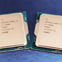 |
by Gavin Bonshor on (#64Y8V)
Today marks the release of Intel’s 13th Gen Core series, codenamed Raptor Lake. The first models to be unleashed into retail channels are all overclockable parts, with six SKUs across the Core i9, i7, and i5 product segments. While we’ve seen Intel’s heterogeneous or hybrid design with the launch of Intel’s Alder Lake (12th Gen Core) products, the latest Raptor Lake core brings a very similar design to the table, but with subtle improvements designed to help give Intel the leading edge in the desktop market.First of these is a ‘new’ Raptor Cove performance (P) core using a refined Intel 7 manufacturing process with some subtle yet critical improvements to the LGA1700 platform to help increase generational performance. Perhaps the most significant benefit comes from adding more efficiency (E) cores, with the flagship SKU, the Core i9-13900K, bringing a total of 24-cores (8P+16E). Which means Intel has effectively doubled the number of efficiency cores on the die.While there are plenty of talking points, ultimately, the proof, or in this case, performance, is in the pudding. With AMD pulling the trigger on its new Zen 4 core built on TSMC’s 5 nm process, does Intel’s 13th generation Core processors have what it takes to go toe-to-toe with the impressive Ryzen 7000? We aim to discover how Raptor Lake shapes up in our review of the Core i9-13900K and the more affordable Core i5-13600K.
|
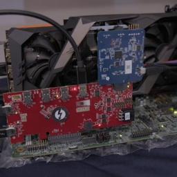 |
by Ganesh T S on (#64X9M)
The DisplayPort 2.1 specifications were officially released by VESA on Monday, and this was followed up by USB-IF's announcement of the release of the 80 Gbps USB4 v2 specifications yesterday. These have have brought to fore the significant engineering efforts put into creating a unified protocol capable of handling the external I/O bandwidth requirements of tomorrow's computing systems. Today, Intel is announcing the demonstration of early prototypes for next-generation Thunderbolt based on the USB4 v2 and DisplayPort 2.1 specifications.Intel's donation of the Thunderbolt 3 specifications to the USB promoters group to form the basis of USB4 has had its share of pros and cons. On one hand, the convergence of the Type-C connector ecosystem theoretically achieved the goal of minimizing end-user confusion, and the royalty-free spec for PCIe tunneling opened up the market to other silicon vendors like ASMedia. However, it also created consumer angst as most of the attractive features of USB4 (such as the 40Gbps bandwidth and compatibility with PCIe tunneling) were entirely optional features. That said, it did enable Intel to market Thunderbolt ports as the Type-C that could do it all. Intel's demonstration of Next Generation Thunderbolt also included a sneak peek into its specifications, even though certain aspects are yet to be finalized. Before delving deeper into Intel's press release, a quick recap of the 80 Gbps USB4 v2 specifications announcement is necessary.USB4 v2 UpdatesUSB4 v2 builds upon the multi-protocol tunneling architecture introduced in USB4 by doubling the available bandwidth while maintaining the same port / pins layout and cable structure. This has been achieved by moving the physical layer signal encoding to PAM3 (described in detail in our coverage of 80 Gbps 'Thunderbolt 5' last year). This means that existing 40Gbps USB4 cables will be able to support 80Gbps operation also.The USB4 v2 specifications now allow tunneling of DisplayPort 2.1 signals and up to four PCIe 4.0 lanes. The data and display protocol updates also make it more efficient, with USB data tunneling capable of exceeding 20 Gbps.One of the key updates in the move to support DisplayPort 2.1 tunneling relates to the maximum total bandwidth for four lanes in UHBR 20 transmission mode. This translates to 80 Gbps, essentially leaving nothing spare on the transmit side for any other protocol. To handle this, USB4 v2 introduces the concept of asymmetric links. In general, a USB4 link uses two bonded high-speed differential signaling pairs to transmit and receive data, allowing for 40 Gbps duplex operation (40 Gbps transmit and 40 Gbps receive) in the symmetric case. However, the lane initialization process can optionally configure the link to have 3 transmitters and one receiver on one side, and 3 receivers and one transmitter on the other. Combined with the higher data rates thanks to PAM3, this can allow the host to send out 120 Gbps, while lowering the receive bandwidth to 40 Gbps. High-resolution displays can be reliably driven without too much of a sacrifice of the bandwidth available on the transmit side for other purposes (like high-speed storage).The power delivery specifications have also been updated to match the updates made in USB4 v2, and new logo guidelines have been issued for consumer-facing equipment.Next-Generation ThunderboltThunderbolt has seen incredible momentum over the last couple of years - triggered mainly by the integration of Thunderbolt controllers inside the high-volume notebook processors starting with Ice Lake. The combination of data, video, and power delivery in one port / cable makes it beneficial to a host of use-cases. In particular, the increasing popularity of hybrid work / hot-desking (monitors / networking etc. behind a dock, allowing multiple employees to just plug in their Thunderbolt-equipped systems at different times) has also served as a fillip to Thunderbolt adoption in the business / office space. Gamers and content creators have an incredible thirst for I/O bandwidth that is served well by Thunderbolt.As mentioned earlier, Next Generation Thunderbolt takes the USB4 v2 specifications as baseline and makes all of the attractive optional features into mandatory ones. On top of this, Intel's integration of Thunderbolt into the notebook processors ensures that the implementation is power efficient on the host side. Making Thunderbolt mandatory for Intel Evo and vPro notebooks further cements Intel's leadership in the USB4 v2 space.The dynamic bandwidth rebalancing feature allowing tunneling of the highest bandwidth DisplayPort 2.1 streams while still allowing usage of high-bandwidth peripherals is one of the most exciting features of USB4 v2 that is sure to be available in systems equipped with the Next Generation Thunderbolt ports.Intel's demonstration included both host and device implementations, with the host configuration shown in the beginning. A discrete GPU's DisplayPort output is fed into the host controller board, and two Type-C cables fork off, one ostensibly to the display, and another to a dock (device) with a SSD attached.Aspects such as power delivery limits (Thunderbolt 3 / 4 support up to 15W by default) for the Next-Generation Thunderbolt ports will be clarified in the near future. Intel did not provide any information related to market availability.Based on a glance through the USB4 v2 specifications and Intel's description of Next-Generation Thunderbolt, it is clear that Thunderbolt ports will continue to remain the Type-C port that does it all.
|
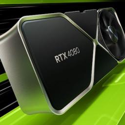 |
by Ryan Smith on (#64QZE)
In a short post published on NVIDIA’s website today, the company has announced that it is “unlaunching” their planned GeForce RTX 4080 12GB card. The lowest-end of the initially announce RTX 40 series cards, the RTX 4080 12GB had attracted significant criticism since it’s announcement for bifurcating the 4080 tier between two cards that didn’t even share a common GPU. Seemingly bowing to the pressure of those complaints, NVIDIA has removed the card from their RTX 40 series lineup, as well as cancelling its November launch.NVIDIA’s brief message reads as follows:
|
 |
by Ryan Smith on (#64QQ7)
As part of this week’s Microsoft Ignite developers conference, Microsoft’s DirectX team has published a few blog posts offering updates on the state of various game development-related projects. The biggest and most interesting of these is an update on DirectStorage, Microsoft’s API for enabling faster game asset loading. In short, the long-awaited 1.1 update, which adds support for GPU asset decompression, is finally on its way, with Microsoft intending to release the API to developers by the end of this year.
|
 |
by E. Fylladitakis on (#64P8D)
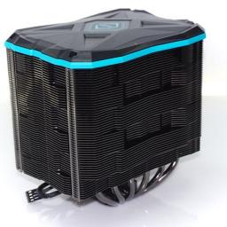
In today's review, we are taking a look at the flagship product of Iceberg Thermal, a relatively new US-based company. The IceSLEET G6 Stealth cooler that we are putting to the test today is a behemoth of a CPU cooler, intended to bring quiet cooling to users who want the very best but without the added complexity of liquid-based coolers.
|
 |
by Anton Shilov on (#64JMT)
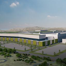
Now that the U.S. government has finally settled the matter of whether it would be providing subsidies to entice chip fabs to setup shop within the U.S., those fabs and chip makers are starting to hammer out their domestic investment plans. Of all of the proposals revealed so far, Micron's new proposal stands to be the most ambitious. Last week the company announced plans to build the largest chip production complex in the history of the U.S. in central New York state. The plan will span 20 years of construction and upgrades, with a total price tag expected to hit around $100 billion by the time Micron is finished in the 2040s.Micron's new site near Clay, New York, will not only be the company's largest campus ever built, but will also be the largest chip fab in the USA. The new Micron campus will produce DRAM using leading-edge process technologies and is expected to eventually include four 600,000 feet (55,700 meters) clean rooms. Which, to provide some context, is roughly eight-times the clean room space of GlobalFoundries' Fab 8. The new fab complex will complement Micron's already announced campus near Boise, Idaho, that is expected to start coming online starting in 2025. Both sites will be instrumental to meet Micron's goal to produce 40% of its DRAM in the U.S. over the next decade.According to Micron, the company's investments in its New York production facility will total $100 billion when fully built, and it will create some 9,000 Micron jobs along with some 41,000 indirect jobs. The first phase of the Clay, New York, project is expected to cost Micron around $20 billion in total over the rest of this decade. The DRAM maker expects to get $5.5 billion in incentives from the state of New York over the life of the project, as well as federal grants and tax credits from the CHIPS and Science Act. In addition, Micron and the state of New York will also invest $500 million over the next 20+ years in community and workforce development.Micron plans to start site preparation work in 2023 and start construction in 2024. The facility ramp up is set to begin in the second half of the decade based on industry demand for DRAM devices.Broadly speaking, fab complexes with eye-popping price tags are quickly becoming the norm in the fab industry as the cost of building and equipping successive generations of fabs continues to balloon. And while Micron is not the first company to plan for a twelve digit price tag for a new fab complex (Intel's new fab complex in Ohio is officially expected to cost around $100 billion when completed), Micron's announcement is notable in that unlike Intel and TSMC, Micron isn't a logic producer. So the company's $100 billion plans are entirely for memory, a relatively bold commitment for a conservative company that's competing in the tech industry's classic commodity market.Bearing in mind that the new fab in in Onondaga County, New York, is not set to come online until the later half of the decade, it is too early for Micro to reveal which process technologies and types of products it will produce. The only thing that the company says is that this will be a leading-edge facility that will produce advanced DRAM products (think 64Gb DDR5 chips, DDR6 DRAMs, next-generation HBM, etc.) using EUV-enabled production nodes."Micron will leverage the diverse, highly educated and skilled talent in New York as we look to build our workforce in the Empire State," said Sanjay Mehrotra, chief executive of Micron. "This historic leading-edge memory megafab in Central New York will deliver benefits beyond the semiconductor industry by strengthening U.S. technology leadership as well as economic and national security, driving American innovation and competitiveness for decades to come."Source: Micron
|
 |
by Anton Shilov on (#64JDW)
Samsung outlined its foundry business roadmap for the next five years at its Foundry Forum event last week. The company plans to introduce its next generation fabrication technologies in a timely manner and intends to make chips on its 1.4 nm (14 angstroms) manufacturing process by 2027. Also, the company will keep investing in new manufacturing capacity going forward as it strives to strengthen its position in the foundry market.New Nodes IncomingSamsung has been introducing new production nodes and/or variants on production nodes every 12 – 18 months for several years now, and plans to keep its rather aggressive pace going forward. Though the company’s roadmap illustrates, fanfare aside, that it is now taking longer to develop new fabrication processes. The company’s second-generation 3 nm-class gate-all-around (3GAP) technology is now set to arrive sometime in 2024. Meanwhile, Samsung Foundry intends to be ready with its 2 nm (20 angstroms) node in 2025, and with its 1.4 nm-branded fabrication process in 2027."With the company's success of bringing the latest [3 nm-class] process technology to mass production, Samsung will be further enhancing gate-all-around (GAA) based technology and plans to introduce the 2 nm process in 2025 and 1.4 nm process in 2027," a statement by Samsung reads.Chip Fab Roadmaps
|
 |
by Ryan Smith on (#64F7P)
Underscoring a difficult second half of the year that seems to be shaping up for the entire tech industry, AMD this afternoon has become the latest tech company to warn investors that revenues for the quarter are going to come in significantly under previous guidance. Releasing a preliminary third quarter financial results statement, AMD is reporting that revenues for the quarter will come in at around $5.6 billion, which is over $1 billion below AMD’s previous guidance of $6.7 billion. Driving this unexpected drop in revenues is an exceptionally weak client market, with revenues down 40% versus Q3’21 and resulting in what’s traditionally AMD’s largest market segment by revenue becoming their smallest.
|
 |
by Ganesh T S on (#64EFH)
Western Digital is introducing a new flagship portable SSD today under the SanDisk Professional brand. The PRO-G40 dual-mode PSSD ticks all the right boxes for prosumers, content creators, and studios looking for a high-performance rugged bus-powered portable storage drive with wide compatibility. We have put the 2TB version of the PRO-G40 through our rigorous direct-attached storage evaluation. Read on to find out how the new PSSD stacks up against the competition.
|
by Ryan Smith on (#645YJ)
With Intel’s annual Innovation event taking place this week in San Jose, the company is looking to recapture a lot of technical momentum that has slowly been lost over the past couple of years. While Intel has remained hard at work releasing new products over the time, the combination of schedule slips and an inability to show off their wares to in-person audiences has taken some of the luster off the company and its products. So for their biggest in-person technical event since prior to the pandemic, the company is showing off as much silicon as they can, to convince press, partners, and customers alike that CEO Pat Gelsinger’s efforts have put the company back on track.Of all of Intel’s struggles over the past couple of years, there is no better poster child than their Sapphire Rapids server/workstation CPU. A true next-generation product from Intel that brings everything from PCIe 5 and DDR5 to CXL and a slew of hardware accelerators, there’s really nothing to write about Sapphire Rapids’ delays that hasn’t already been said – it’s going to end up over a year late.But Sapphire Rapids is coming. And Intel is finally able to see the light at the end of the tunnel on those development efforts. With general availability slated for Q1 of 2023, just over a quarter from now, Intel is finally in a position to show off Sapphire Rapids to a wider audience – or at least, members of the press. Or to take a more pragmatic read on matters, Intel now needs to start seriously promoting Sapphire Rapids ahead of its launch, and that of its competition.For this year’s show, Intel invited members of the press to see a live demo of pre-production Sapphire Rapids silicon in action. The purpose of the demos, besides to give the press the ability to say “we saw it; it exists!” is to start showing off one of the more unique features of Sapphire Rapids: its collection of dedicated accelerator blocks.Along with delivering a much-needed update to the CPU’s processor cores, Sapphire Rapids is also adding/integrating dedicated accelerator blocks for several common CPU-critical server/workstation workloads. The idea, simply put, is that fixed function silicon can do the task as quickly or better than CPU cores for a fraction of the power, and for only a fractional increase in die size. And with hyperscalers and other server operators looking for big improvements in compute density and energy efficiency, domain specific accelerators such as these are a good way for Intel to deliver that kind of edge to their customers. And it doesn’t hurt either that rival AMD isn’t expected to have similar accelerator blocks.
 |
by Gavin Bonshor on (#644AX)
With a lot of news and info dropping on Intel's latest Z790 chipset using the LGA1700 socket, NZXT has pulled the trigger and announced its N7 Z790 motherboard. Available in either white or black, it features a 2.5 GbE controller, Wi-Fi 6E CNVi, benefits from support for PCIe 5.0, and includes three M.2 slots.In addition to the announcement of Intel's 13th Gen Core series processors, codenamed Raptor Lake, NZXT has announced its plans to launch the N7 for Z790. As we've seen from NZXT motherboards in the past, the N7 Z790 has a large swathe of armor covering the board and is available in both back and white color schemes. It should be noted that neither the black nor white model includes any integrated RGB LED lighting. Typical with an NZXT product, the N7 Z790 comes with support with their CAM software.Some of the NZXT N7 Z790's main features include one full-length PCIe 5.0 x16 slot, two full-length PCIe 4.0 slots operating at x4/x4, and two PCIe 3.0 x1 slots. Also present on the NZXT N7 Z790 are three M.2 slots, two with support for PCIe 4.0 x4 NVMe drives and one with support for both PCIe 4.0 x4 and SATA. NZXT also includes four SATA ports with support for RAID 0, 1, 5, and 10 arrays for more conventional storage. NZXT is also advertising support for DDR5-6000 memory, with a combined total of 128 GB supported across four slots.NZXT is also advertising a 16+1+2-phase power delivery, with one 8-pin EPS 12 V and one 4-pin 12 V power connector pairing to deliver power to the CPU. Powering the rest of the board's components is a 24-pin 12V power connector.The rear I/O is modest yet practical, with two USB 3.2 G2 Type-A and three USB 3.2 G1 Type-A; interestingly, NZXT doesn't include any rear panel Type-C connectivity. Also on the rear panel are five 3.5 mm audio jacks and one S/PDIF optical output powered by a Realtek ALC1220 HD audio codec, with two antenna ports for an unspecified Wi-Fi 6E CNVi. Finishing off the rear panel is a single HDMI TM video output, with one Realtek RTL8125BG 2.5 GbE controller.Gallery: NZXT Unveils N7 Z790 Motherboard for Intel 13th Gen CoreThe NZXT N7 Z790 is scheduled to release with an MSRP of $300 and will be available in Q4 2022 in the USA. NZXT hasn't shared whether or not this will be released in other regions.Source: NZXT
|
 |
by Gavin Bonshor & Ryan Smith on (#643Z4)
It's time again for another Intel event, Intel Innovation 2022. With plenty of tech things to reveal to the world ranging from AI, client computing, and data center/cloud computing. Intel is also expected to showcase the generation of products for consumers.With AMD's big Ryzen 7000 launch having only taken place just yesterday, Intel is expected to showcase its next generation of products for consumers. Leading the keynote will be visionary Intel CEO Pat Gelsinger.The live blog will start with the opening keynote from Intel Innovation at 9am PT / 16:00 UTC / 18:00 CEST.
|
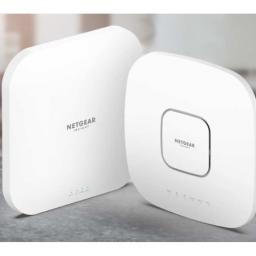 |
by Ganesh T S on (#643QE)
Netgear has been at the forefront of the SDVoE (Software-Defined Video over Ethernet) initiative with multiple AV switches serving the growing market. The ProAV lineup of managed switches have been sold primarily in a B2B setting by the Netgear Business division. These switches are increasingly becoming part of luxury residential installations requiring an AV-over-IP solution. As part of the CEDIA Expo 2022, Netgear is announcing a new 'Netgear Home Solutions' push. The intention is to take the same lineup of Netgear AV products sold by Netgear Business and target it towards both commercial and residential installations.As part of this initiative, Netgear will be selling ProAV Managed Switches and ProWiFi Access Points to residential installers, along with the Pro version of Insight Remote Management and Pro Support. While the ProAV Managed Switches are already in the market, the new WAX628 and WAX638E APs are complementary to the currently existing members of the Insight Access Point Portfolio.The WAX628 (already available for residential installers) slots in-between the dual-band AX3600 WAX620 and the tri-band AX6000 WAX630. This AX5400 dual-band solution supports 160 MHz channel bandwidth, and is accompanied by the AX7800 WAX638E which adds 6 GHz band support to the mix. The Wi-Fi 6E AP is slated to come to the market in the next few months.Netgear is promising margin protection for installers by selling the ProAV and ProWiFi products only through the channel and not via Amazon or other e-tailers. Since these products are going to reach end-consumers through custom installers who have their own cost structures, the lack of any pricing information from Netgear is not surprising.Netgear's traditional consumer Wi-Fi router market has evolved rapidly over the last few years. Despite the success of Orbi (in both the consumer and SMB markets), new entrants like eero have gained significant mind and market share. In this context, Netgear has to look towards services and expand into new markets in order to maintain and build upon their technical leadership. Forays into lucrative niches like the residential installer market are not surprising.Gallery: Netgear Introduces Wi-Fi 6 / 6E Access Points and Services for Residential Installers
|
 |
by Ryan Smith & Gavin Bonshor on (#642FC)
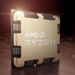
During AMD’s ‘together we advance_PCs’ event at the end of August, the company unveiled its Ryzen 7000 series of desktop processors, with four SKUs aimed at the mid-range and high-end market segments. After whetting the audience's appetites with that announcement, tomorrow AMD will be officially releasing their long-awaited next-generation CPUs.The launch of the Ryzen 7000 series brings a lot to digest, for casual fans and hardcore hardware enthusiasts alike. For their newest lineup of chips, AMD has given their desktop CPU platform a top-to-bottom update, not only releasing new CPUs, but releasing an entirely new platform, socket AM5 around it. As a result, for the first time in a few generations these chips are not drop-in compatible with existing AMD motherboards. But at the same time it has allowed AMD to deliver on a collection of platform improvements, ranging from DDR5 and PCIe 5.0 support to improved power management capabilities. AMD has even managed to sneak an entry-level Radeon RDNA2 architecture-based iGPU into the chip.
|
 |
by Ganesh T S on (#63XYY)
Intel officially unveiled the final member of their Alder Lake-based NUC12 family earlier this week. The NUC12 Enthusiast (like the three previous Enthusiast NUCs) caters to the gaming / creators market looking for a small form-factor machine with a discrete GPU.As a refresher, Intel created the NUC Enthusiast category back in 2016 with the introduction of the Skull Canyon NUC (NUC6i7KYK). With a 4" x 5" motherboard, it had a slightly larger footprint compared to the traditional NUCs. However, the increased size allowed the incorporation of a 45W TDP processor with increased graphics flex. The second generation Hades Canyon moved to a slightly larger board (5.5" x 8"), while retaining the industrial design of the Skull Canyon NUC. It used the Kaby Lake-G processors with a Kaby Lake processor and an AMD GPU packaged together (with a total TDP budget between 65W and 100W). The NUC11 Enthusiast (Phantom Canyon) went for a more traditional gaming notebook-type architecture with a Tiger Lake-U Core i7-1165G7 and a NVIDIA RTX 2060 laptop GPU.The NUC12 Enthusiast retains a similar architecture. The key difference lies in the fact that this is first NUC to utilize Intel's Arc discrete GPU. The specifications of the GPU are much more powerful than the NVIDIA RTX2060, and this has resulted in a redesign of the cooling solution as well as the chassis dimensions compared to the NUC11 Enthusiast.Similar to the Phantom Canyon family, Serpent Canyon will also come in two varieties - a barebones version, and another with a 1TB SSD / 16GB of DDR4-3200 RAM / Windows 11 Home pre-installed. The SKUs utilize the Intel Core i7-12700H notebook processor and the Intel Arc A770M discrete GPU with 16GB of VRAM.The NUC12 Enthusiast sports a rich set of I/Os. There are two Thunderbolt 4 ports (one in the front and one in the rear) that also carry the display output from the Intel Iris Xe Graphics in the Core i7-12700H. Two USB 3.2 Gen 2 Type-A ports and a SDXC UHS-II slot, along with an audio jack and a quad-microphone array round out the front panel. On the rear, we have an audio output jack (supporting TOSLINK), a single 2.5 Gbps LAN port, four USB 3.2 Gen 2 Type-A ports (with a hub chip behind), and the display outputs (1x HDMI 2.1 4Kp60 and 2x Display Port 2.0 (1.4 certified)) from the Intel Arc A770M.The table below compares the specifications of the flagships in the last three generations of Enthusiast NUCs.Intel Enthusiast NUCsModelSerpent Canyon
|
 |
by Gavin Bonshor on (#63VT6)
Even though the main focus this month has been on AMD's upcoming launch of its Ryzen 7000 desktop series processors based on the Zen 4 architecture, AMD is also in the process of launching its 7020 series of processors designed for entry-level mobile, codenamed Mendocino. It has launched four new SKUs for mobile, including two Ryzen series models and two Athlon variants, all based on its Zen 2 architecture.As we learned in May, AMD's Zen 2 based 'Mendocino' APUs are designed as part of its lower-end mobile processor stack for entry-level thin notebook and laptop solutions. The affordable APUs incorporate up to 4 Zen 2 CPU cores, as well as AMD's integrated Radeon 610M graphics, all with a maximum TDP of 15W.Focusing specifically on the AMD 7020 series APUs announced today, the top SKU is the Ryzen 5 7520U. Using AMD's new Ryzen Mobile CPU numbering system, the 7520U is a model year 2023 chip under the Ryzen 5 series banner using its Zen 2 core architecture. The U suffix technically means 15-28W, but in this case AMD has confirmed that all of the current chips have a max TDP of 15W.The AMD Ryzen 5 7520U benefits from a 2.8 GHz base frequency across its four cores, with a 1T boost frequency of up to 4.3 GHz. It also includes a total of 6MB of cache, split between 4MB of L3 and 2MB of L2 (512KB per core).AMD Ryzen 7020 Series (Mendocino) LineupSKUCores/ThreadsCPU Frequency
|
 |
by Ryan Smith on (#63VHT)
With NVIDIA’s fall GTC event in full swing, the company touched upon the bulk of its core business in one way or another in this morning’s keynote. On the enterprise side of matters, one of the longest-awaited updates was the shipment status of NVIDIA’s H100 “Hopper” accelerator, which at introduction was slated to land in Q3 of this year. As it turns out, with Q3 already nearly over H100 is not going to make its Q3 availability date. But, according to NVIDIA the accelerator is in full production, and the first systems will be shipping from OEMs in October.
|
 |
by Ryan Smith on (#63VEE)
Among the spate of announcements from NVIDIA today as part of their fall GTC 2022 event, the company is delivering a surprising shake-up to their DRIVE automotive SoC plans. Effective immediately, NVIDIA has cancelled Atlan, their planned post-Orin SoC for 2025 automobiles. In its place, NVIDIA is announcing Thor, an even more powerful SoC set to launch in the same 2025 timeframe.
|
 |
by Ryan Smith & Gavin Bonshor on (#63V3D)
Kicking off a bit later this morning will be NVIDIA’s GTC 2022 fall keynote, which should prove to be a very interesting event.Besides NVIDIA’s usual run-through of business announcements, the first part of this GTC’s keynote will be focused on NVIDIA’s GeForce products, making for a very rare appearance at NVIDIA’s increasingly enterprise-focused event. NVIDIA has been teasing the GeForce portion of the event as “Project Beyond” for about the past month, and in traditional secretive NVIDIA fashion, that’s all we officially know ahead of the show.Given the timing of this event, the announcement of NVIDIA’s next-generation of consumer video cards (GeForce RTX 40 series?) and associated GPUs is a very safe bet. The GeForce RTX 30 series premiered just over two years ago, which is right in line with NVIDIA’s usual bi-yearly architecture cadence.Significant performance improvements are (hopefully) in the cards, but it will be interesting to see what NVIDIA does in light of the current cypto hangover, which hit a fevered pitch last week with the long-awaited completion of the Ethereum Merge – eliminating the need for video cards to mine the popular cryptocoin. The market for video cards is almost certain to be saturated for the next several months, especially as the performance levels covered by the current RTX 30 series cards. Which means it’s cards that would be faster than the RTX 3090 and its ilk that are the most likely to succeed in the current climate.At the same time, from a graphics feature standpoint NVIDIA has been relatively stagnant since the release of the Turing architecture (RTX 20 series) in 2018, when NVIDIA first added DirectX 12 Ultimate (FL 12_2) support. As a result, a more feature-focused release would not be unusual for NVIDIA, but at the same time we’re not immediately aware of any new features under development for DirectX.Following CEO Jensen Huang’s GeForce presentation, we’re expecting the GTC keynote to then dovetail into a more traditional enterprise presentation. NVIDIA’s H100 Hopper accelerator will no doubt be a big focus, as it’s slated to ship soon. As well, NVIDIA has been ever-increasingly focused on robotics, medical, automotive, and of course their omniverse simulation environment. So there should be no shortage of other things to talk about – even if we’re here first and foremost for the gaming cards.NVIDIA's keynote starts at 8am Pacific (15:00 UTC), so please join us for our live blog coverage of the green machine’s latest announcements.
|
 |
by Ryan Smith on (#63QR0)
While we’re still over a quarter out from the end of 2022, Intel already has its eyes aimed at 2023 and its eventual refresh of its mobile processors. To that end, today the company has announced that they are making some branding changes for the low-end.Starting in 2023, Intel will be retiring the Pentium and Celeron brands for laptop processors. In its place, Intel will have a singular “Intel Processor” brand for the low end of the market, while the Core branding (with its multiple tiers) will remain in place for the rest of Intel’s mobile product stack.“Whether for work or play, the importance of the PC has only become more apparent as the torrid pace of technological development continues to shape the world. Intel is committed to driving innovation to benefit users, and our entry-level processor families have been crucial for raising the PC standard across all price points. The new Intel Processor branding will simplify our offerings so users can focus on choosing the right processor for their needs.”-Josh Newman, Intel vice president and interim general manager of Mobile Client PlatformsNotably, this change only applies to future laptop parts. At this point Intel is not announcing a change for desktop parts or embedded parts. But with that said, I would not be the least bit surprised if these change ultimately came to desktops as well, as mobile is effectively Intel’s leading consumer market segment these days. So technology and names tend to percolate up to the desktop segment, keeping the two in sync.Intel’s current generation Pentium and Celeron offerings are both based on Alder Lake-U processors with a single performance core and four (one block of) efficiency cores. The only differences between these SKUs, besides price, is clockspeeds – specifically, that the Celeron parts lack turbo. So if Intel is going to pursue a similar strategy in future generations, then it’s not outlandish to fold two similar products under a single brand. Though the decision to forgo any kind of specific branding is an unusual one for Intel.With that said, there’s also been a notable absence of “pure” Atom parts in this segment in this generation. Intel has yet to produce a true entry-level part using its Gracemont Atom cores; so everything below the Alder Lake Pentiums/Celerons has been the last-generation Tremont Atoms. So larger changes may be afoot for Intel’s cheapest laptop product segment.
|
 |
by Ryan Smith on (#63QQ9)
In a move that will have significant repercussions for the video card industry in North America and Europe, EVGA today has announced that the company is parting ways from NVIDIA. As a result, the company will not be producing video cards based on NVIDIA’s next-generation of GPUs – and won’t be immediately switching allegiance to AMD or Intel, either. Consequently, NVIDIA is losing their largest add-in board (AIB) in North America, and the broader North American video card market is losing one of its biggest and best-known vendors.In a brief announcement posted on EVGA’s forums, the company outlined their parting from NVIDIA, while underscoring that this affects the next-generation of video cards, and that EVGA will continue to provide current-gen products and support existing customers.
|
 |
by E. Fylladitakis on (#63PY3)
In today's review, we are taking a look at a tiny beast, the FSP Dagger Pro 850W power supply. Although reduced to standard SFX proportions and forced to use a low-profile 92 mm fan, FSP's engineers managed to pull 850 Watts out of this miniature power plant.
|
 |
by Ryan Smith on (#63NGZ)
Just under four years ago, Arm announced their Neoverse family of infrastructure CPU designs. Deciding to double-down on the server and edge computing markets by designing Arm CPU cores specifically for those markets – and not just recycling the consumer-focused Cortex-A designs – Arm set about tackling the infrastructure market in a far more aggressive manner. Those efforts, in turn, have increasingly paid off handsomely for Arm and its partners, whom thanks to the likes of products like Amazon’s Graviton and Ampere Altra CPUs have at long last been able take a meaningful piece of the server CPU market.But as Arm CPUs finally achieve the market penetration that eluded them in the previous decade, Arm needs to make sure it isn’t resting on its laurels. Of the company’s three lines of Neoverse core designs –the efficient E, flexible N, and high-performance V – the company is already on its second generation of N cores, aptly dubbed the N2. Now, the company is preparing to update the rest of the Neoverse lineup with the next generation of V and E cores as well, announcing today the Neoverse V2 and Neoverse E2 cores. Both of these designs are slated to bring the Armv9 architecture to HPC and other server customers, as well as significant performance improvements.
|
 |
by Anton Shilov on (#63M7V)
Micron this week broke ground on its leading-edge memory production facility near Boise, Idaho. The company will invest $15 billion in its new fab as a part of its ambitious plan to invest $40 billion in its U.S.-based manufacturing capacities by the end of this decade as well as spend $150 billion on new fabs by 2030 globally.Micron's upcoming leading-edge fab will produce DRAM and will be a rather colossal manufacturing facility. At build-out, when the fab is fully equipped with tools, its cleanroom space will reach 600,000 feet (55,700 meters), which is about two times larger compared to cleanroom space at GlobalFoundries' Fab 8 and which is comparable to cleanroom space at giant fabs operated by Micron's rivals Samsung and SK Hynix is South Korea. Essentially, Micron will operate one of the largest semiconductor production facilities in the U.S.The new fab will be located adjacent to Micron's R&D center and headquarters near Boise, Idaho, which will bring together scientists, process technology developers, and manufacturing engineers in one location, something that promises to speed up time-to-yield and time-to-market for advanced DRAMs."With this facility, Micron will closely couple R&D and manufacturing, providing synergies that will enable us to accelerate the production ramp of advanced memory technology," said Sanjay Mehrotra, president and CEO of Micron.Micron is currently prepping the site for the new fab and plans to begin construction in early 2023 in a bid to start bringing cleanroom space online gradually starting in 2025. The facility will be equipped with modern deep ultraviolet (DUV) and extreme ultraviolet (EUV) lithography tools and will make memory using one of Micron's advanced EUV-enabled production nodes. The company intends to start fabbing DRAMs at its new facility sometimes in 2025 and then ramp up production to the full capacity in the following years.At present it is hard to guess which fabrication process will be adopted at the new fab. Considering the fact that Micron is expected to start DRAM production using its first EUV-enabled manufacturing technology (1γ) sometimes in mid-2023 – early-2024, it is likely that the fab near Boise, Idaho, will adopt the company's second EUV-enabled process (1δ). Yet, this is an educated guess (based on habitual introduction of new DRAM nodes every 18 months or so) at this point.Micron intends to make 40% of its global DRAM output in America in 2030s, a rebalance that the company has not done in decades. Therefore, in addition to Micron's new fab near Boise, Idaho, the company plans to build a yet another DRAM facility in the U.S. Currently the company is in the final stages of its selection process for another site in America.Micron will invest $15 billion in the new manufacturing facility near Boise, Idaho. The company also plans to get incentives from the local and state authorities and support from the federal government enabled by the CHIPS and Science act signed into law last month."The investment, made possible by the anticipated grants and credits provided by the CHIPS and Science Act, also enhances Micron's supply chain resilience and will establish a new strategic capability for the U.S.," said the head of Micron.It is noteworthy that Micron is not the only DRAM maker to start building new memory fabs when demand for both 3D NAND and DRAM is down. Last week SK Hynix began to expand its M15 site with its new M15X building as the company is preparing for increased DRAM demand starting in 2025.Source: Micron
|
 |
by Gavin Bonshor on (#63F2F)
In preparation for AMD's Ryzen 7000 series processors, which will launch on September 27th, ASRock has announced that it has developed a new BIOS for its AM5 motherboards. ASRock states that its new firmware has been built to decrease booting times on its motherboards.With every new platform, chipset, and processor launch, firmware is one of the focal points surrounding motherboards. Over the last couple of years, leading vendors such as ASUS, GIGABYTE, and MSI have kept their firmware consistent, regardless of whether the board is designed for AMD or Intel. ASRock has announced that it has developed a new BIOS specifically for its AM5 motherboards, which are designed to support the upcoming AMD Ryzen 7000 series Zen 4 processors based on TSMC's 5 nm process node.
|
 |
by Gavin Bonshor on (#63DX1)
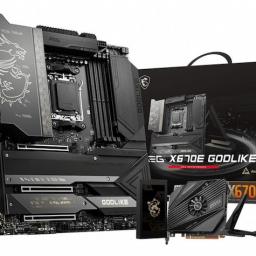
Ahead of the launch of AMD's latest Ryzen 7000 processors, which will hit retail shelves on September 27th, MSI unveiled pricing on four of its X670/X670E motherboards. Given the world's current financial climate and features such as PCIe 5.0 connectivity to M.2 storage drives and at least one PCIe x16 slot, the writing has been on the wall for a while regarding pricing.Currently listed in their US store, MSI has two premium (MEG), one mid-range (MPG), and one entry-level regular X670 (Pro) model, with prices ranging from $290 (Pro X670-P WIFI) up to $1300 (MEG X670E Godlike).
|
 |
by Anton Shilov on (#63DFE)
When a major South Korean memory firm invests over $11 billion in a fab, that raises a couple of eyebrows. But when it comes within a major $100+ billion capital expenditure (CapEx) package, it certainly warrants some attention.Semiconductor business in general and memory business in particular are very cyclical in their nature. Just a year ago almost all chips were in short supply and prices of commodities like memory or display drivers were high, but now that sales of PCs are declining, memory prices are declining too. But several years down the road demand for PCs and other client devices will rise once again, and so will demand for memory. Which is why SK Hynix is already preparing for this with its Fab M15X expansion plan.SK Hynix’s Fab M15X will be a two-story building occupying 60,000 m of land and will be located adjacent to existing Fab M15 in the Cheongju Technopolis industrial complex. The fab will produce 3D NAND (which means more chemical vapor deposition and etching tools in the cleanroom) and/or DRAM (which is more lithography-intensive, so more DUV and EUV equipment in the cleanroom) memory chips, depending on demand by the time it comes online sometimes in 2025. Since at present it is unclear/undecided what the fab will produce, the company cannot disclose planned production capacity of the upcoming manufacturing facility.At a planned size roughly equal to combined space of SK Hynix’s existing Fab M11 and Fab M12, the company’s Fab M15X expansion looks more like an entirely new fab built adjacent to existing Fab M15 than an expansion project of the existing fab. Yet since the two manufacturing facilities share infrastructure and various facilities, the maker prefers to call it Fab M15X."Looking back on the past 10 years, SK hynix could grow into a global company as it boldly carried out investment during crisis," said Park Jung-ho, vice chairman and co-chief executive of SK Hynix. "As we look to prepare for the next 10 years now, I believe starting the M15X will be a first step to lay foundation for a solid future growth."Source: SK Hynix
|
 |
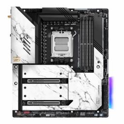
by Gavin Bonshor on (#63D1S)
As we near the end of Intel's 12th Gen (Alder Lake) life cycle, its 13th Gen Core series is expected to be due by the end of the year; we're looking at a premium model from the Z690 chipset. As we already know, Intel's Z690 chipset (LGA 1700) will offer support for the impending 13th Gen Core series, so it does offer a viable upgrade path for users looking to build a 12th Gen Core series system today and potentially upgrade at a later date.Today's model on the test bench is the MSI MPG Z690 Carbon WIFI with a solid feature set that includes 2.5 GbE and Wi-Fi 6E networking, two full-length PCIe 5.0 capable slots, four PCIe 4.0 x4 M.2 slots, as well as a large 19-phase power delivery. The MPG Z690 Carbon WIFI is positioned in the mid-range segment of the market, but at the $350-400 price point, MSI does have some stiff competition. It's time to see how the Z690 Carbon WIFI stacks up and if its gaming-focused model below its enthusiast-level MEG series can deliver the goods.
|
 |
by Ryan Smith on (#63BW3)
It's that time of the year again - Apple's fall iPhone event, where we expect the Cupertino company to unveil its newest generation family of iPhones - what should be the iPhone 14 series.With Apple seemingly satisfied with its current industrial design as embodied by the iPhone 13 lineup, it will be interesting to see what the company does to iterate on its flagship phones this year – especially the high-end Pro designs. In which case, this year may be all about the guts, and what Apple does to update things like the cameras and displays.Meanwhile, it's all but assured that Apple will introduce a new generation processor in the form of the A16. Apple's latest iterations of SoC silicon have been ground-breaking and industry leading, and we expect the new chip to once again push the envelope in performance and efficiency, as Apple is wont to do.The live blog will start along with the event at 10am PT / 17:00 UTC / 19:00 CEST.
|
 |
by Ryan Smith on (#63BPM)
While all eyes are on the impending launch of AMD’s new Ryzen 7000 desktop processors, the chipmaker also has its wheels in motion for the future of its mobile product lineup. And while we’re still quite a bit away from the first Zen 4 mobile parts, more immediate on AMD’s roadmap is their Zen 2-based Mendocino SoC, which is aimed at mainstream laptops. Mendocino APUs are set to launch next quarter, and to prepare for that launch, AMD today is updating their mobile processor numbering scheme to accommodate those future products.The short version of matters is that while the new numbering system is quite similar to AMD’s previous system (e.g. Ryzen Mobile 6000), the company is now dedicating a digit to represent the version of the Zen architecture used. With AMD set to have Zen 2 (Mendocino), Zen 3 (Rembrandt), and eventually Zen 4 (Phoenix) mobile APUs all on the market at the same time, AMD has decided that they need to better disclose the architecture used underneath – a “necessary evil”, as former AnandTech CPU editor Dr. Ian Cutress put it, to avoid any improprieties (perceived or otherwise) that AMD is misleading customers by offering multiple versions of the Zen architecture.
|
 |
by Ryan Smith on (#63AG2)
Qualcomm this morning is taking the wraps off a pair of new SoCs for the mid-range and entry-level smartphone markets. Refreshing the company’s longstanding 600 and 400 series of chips, Qualcomm is announcing the Snapdragon 6 Gen 1 and Snapdragon 4 Gen 1. Both SoCs are receiving similar spec bumps, incorporating newer and faster IP blocks from Qualcomm – such as Arm Cortex-A78 derived CPU cores – as well as moving to newer, more contemporary manufacturing processes.The Snapdragon 600/400 lineups were last updated in mid and early 2021 respectively, so as Qualcomm is already preparing for 2023, the time has finally come to update the bottom half of their product stack. Following Qualcomm’s broad cascading IP strategy, this generation of parts sees both SoC lineups migrate to Cortax-A78 CPUs for their main CPU cores, and in the case of the 6 Gen 1, doubling the number of high-performance CPU cores. Both SoCs also come with faster Adreno GPUs, though in traditional Qualcomm fashion, the company isn’t offering much in the way of details on the underlying hardware there.Notably, however, Qualcomm’s 2023 mid-range/low-end parts aren’t making the jump to the Armv9 architecture. Unlike the 8 Gen 1 and 7 Gen 1, which incorporated Arm’s new Armv9 cores, Qualcomm’s cascading development strategy means that the 6 and 4 series will remain a bit farther behind the curve. For end users this should have little significance for the moment, but for smartphone vendors and software developers, it does mean Qualcomm won’t complete the Armv9 transition for at least another generation.Meanwhile, coming up on nearly a year since Qualcomm announced their initial Snapdragon 8 Gen 1 SoC, today’s announcement from Qualcomm brings their remaining smartphone SoC families in alignment with their new product branding strategy. The 6 and 4 series pick up from where the 600 and 400 series left off, respectively, resetting the counted with the inaugural Gen 1 parts. Like the rest of simplified “Gen” series, this also means that Qualcomm is doing away with individual model numbers for its Kyro/Hexagon/Adreno/Spectra blocks, obfuscating a bit what generation of IP Qualcomm is using there.
|
 |
by Brett Howse on (#63515)
MSI is synonymous with gaming notebooks and the company’s Raider lineup is one of the top gaming platforms on the market. But, MSI has always kept a tiny bit back, reserving their most interesting ideas and most powerful configurations for their Titan lineup.MSI’s Titan series always offers something special. Something different. Something unique. Look back to the insane MSI GT80 Titan from 2015 which featured a full desktop keyboard melded onto an 18.4-inch notebook computer. The MSI GT76 Titan packed in a full desktop Core i9-9900K processor into a more traditional 17-inch form factor.Today we are looking at the latest iteration from MSI; the Titan GT77. Featuring a desktop-inspired Core i9-12900HX processor and an NVIDIA RTX 3080 Ti Laptop GPU, the GT77 is one of the most powerful notebooks on the market today.
|
 |
by Gavin Bonshor on (#632WX)
During AMD's 'together we advance_PCs event, the company unveiled its latest Zen 4-based Ryzen 7000 processors to the world, as well as its AM5 platforms, including X670E, X670, B650E, and B650. AMD also announced what it calls AMD EXPO, a new technology for overclocking DDR5 memory. In conjunction with this announcement, AMD has partnered with memory manufacturers including ADATA, Corsair, G.Skill, GeIL, and Kingston Technology to bring AMD Ryzen 7000 optimized kits of DDR5 memory to the market, with 15 (or more) of these set to be available on launch day on September 27th.AMD EXPO stands for EXtended Profiles for Overclocking and is designed to provide users with high-end memory overclocking when used in conjunction with AMD's Ryzen 7000 series processors. Similar to Intel's preexisting X.M.P (Extreme Memory Profile) technology found on most consumer-level memory kits designed for desktop Intel platforms, AMD's EXPO technology aims to do the same, but as an open standard with an emphasis on providing the best settings for AMD platforms.AMD EXPO Technology: Like X.M.P, but Optimized for Ryzen 7000The premise of AMD EXPO is that it will be a one-click DDR5 overclocking function for AM5 motherboards, and AMD claims that EXPO overclocked memory kits will offer up to 11% higher gaming performance at 1080p, although it hasn't quantified how it came to this figure. AMD did, however, state that it is expecting (at least) 15 kits of DDR5 memory with AMD EXPO at launch on September 27th, with rates of up to DDR5-6400.AMD EXPO, on the surface, is essentially an X.M.P profile specifically designed for AMD's Ryzen 7000 (Zen 4) processors. Although AMD hasn't gone into finer details on how it differs from X.M.P, beyond the fact that it will be royalty and licensing fee free.
|
 |
by Gavin Bonshor on (#631P9)
Over the last couple of months, the rumor mill surrounding AMD's impending Ryzen 7000 processors for desktops has been in overdrive. Although Lisa Su unveiled Zen 4 back at CES 2022, it's been anticipated that the new AM5 platform would include multiple chipsets, much like AM4 has over 500+ motherboard lifespan from X370, X470, X570, and every chipset in between.AMD announced its X670E, X670, and B650 chipsets during the AMD Keynote at Computex 2022, and this evening, AMD has announced a fourth chipset for Ryzen 7000, the B650E chipset. The B650E chipset will run alongside the already announced B650 chipset, but as it's part of AMD's 'Extreme' series of chipsets, it will benefit from PCIe 5.0 lanes to at least one M.2 slot, as well as optional support for PCIe 5.0 to a PCIe graphics slot, features not available with standard B650 boards.During AMD's Keynote at Computex 2022, AMD's CEO Lisa Su unveiled three AM5 chipsets designed to harness the power of its 5 nm Zen 4 cores within the Ryzen 7000 processors. We already knew the AM5 socket was based around a Lane Grid Array (LGA) socket with 1718 pins, aptly named LGA1718. Some of the significant benefits coming to AM5 include native PCIe 5.0 support from the CPU, not just for use with the PCIe slots, but also in the way of PCIe 5.0 storage, where the first consumer drives are expected to start rolling out in November 2022.AMD's latest announcement of the B650E (Extreme) chipset gives motherboard vendors and users the option of a lower-cost platform but without sacrificing the longevity and expansion support of PCIe 5.0. The X670E chipset is reserved for its most premium models, such as the flagship ASUS ROG Crosshair X670E Extreme motherboard, unveiled at Computex 2022.AMD AM5 Chipset ComparisonFeatureX670EX670B650EB650CPU PCIe (PCIe)5.0 (Mandatory)
|
 |
by Ryan Smith on (#631PA)
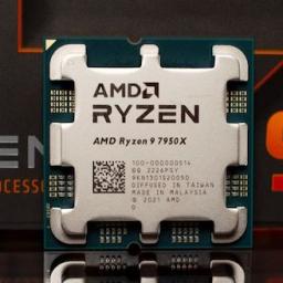
AMD’s "together we advance_PCs”l ivestream presentation just wrapped up moments ago, where AMD CEO Dr. Lisa Su set the stage for the release of the next generation of AMD Ryzen desktop CPUs. Building off of AMD’s Ryzen 7000 announcement back at Computex 2022, the eagerly anticipated presentation laid out AMD’s launch plans for their first family of Zen 4 architecture-based CPUs, which will see AMD kick things off with a quartet of enthusiast-focused chips. Topping out with the 16 core Ryzen 9 7950X, AMD’s Ryzen 7000 chips will be launching in just over 4 weeks’ time, on September 27, with AMD expecting to handily retake the performance crown across virtually all categories of the PC CPU space, from gaming to content creation.Driving AMD’s gains in this newest generation of desktop CPUs is a combination of architectural improvements underpinning the Zen 4 architecture, as well as moving production of the CPU core chiplets to TSMC’s leading-edge 5nm process. The combination of which will allow AMD to deliver what they are saying is now a 13% increase in IPC over their Zen 3 architecture – up from an 11% claim as of Computex – as well as a sizable increase in CPU clockspeeds. The top-end Ryzen 9 7950X will have a maximum turbo clockspeed of 5.7GHz, 800MHz (16%) higher than the equivalent Ryzen 9 5950X. As a result, AMD expects to deliver a 29% generational increase in single-threaded performance, and even more in multi-threaded workloads.
|
 |
by Gavin Bonshor on (#631BJ)
At long last the date is here. AMD this evening will be broadcasting their "together we advance_PCs” event, which will be focused around the upcoming launch of their next-generation Ryzen 7000 processors.AMD first unveiled their Ryzen 7000 platform and branding back at Computex 2022, offering quite a few high-level details on the forthcoming consumer processor platform while stating it would be launching in the fall. The new CPU family will feature up to 16 Zen 4 cores using TSMC's optimized 5 nm manufacturing process for the Core Complex Die (CCD), and TSMC’s 6nm process for the I/O Die (IOD). AMD has not disclosed a great deal about the Zen 4 architecture itself, though their Computex presentation has indicated we should expect a several percent increase in IPC, along with a further several percent increase in peak clockspeeds, allowing for a 15%+ increase in single-threaded performance.The Ryzen 7000 series is also notable for being the first of AMD’s chiplet-based CPUs to integrate a GPU – in this case embedding it in the IOD. The modest GPU allows for AMD’s CPUs to supply their own graphics, eliminating the need for a discrete GPU just to boot a system while, we expect, providing enough performance for basic desktop work.Tonight's presentation, in turn, should finally see AMD moving on to talking about launch details for the Ryzen 7000 CPUs and the associated AM5 platform. That should include performance expectations and a bit more on the motherboards. And, of course, information on the specific chip SKUs that will be hitting the market, including core configurations, clockspeeds, and prices. With any luck we may get a bit more on the Zen 4 architecture as well, as alongside CEO Dr. Lisa Su, CTO Mark Papermaster is slated to present part of the event.The event is set to kick off tonight, August 29, at 7pm ET (23:00 UTC). So be sure to join us for our live blog coverage around the announcement of the next generation of AMD desktop CPUs.
|
 |
by E. Fylladitakis on (#62WXW)
Today we are having a look at the new XG Plus Platinum series, the latest power supply family from prolific PC peripherals producer Cooler Master. Designed to offer a quality PSU with an extra dash of flair, the RGB fan (and RGB display) equipped XG Plus Platinum is a PSU that's not quite like anything else on the market. The XG family ranges from 650 to 850 Watts, and today we're evaluating the most powerful unit in the series, the 850W XG850 Plus Platinum.
|
 |
by Anton Shilov on (#62W32)
Intel this week introduced its new Semiconductor Co-Investment Program (SCIP) under which it will build new manufacturing facilities in collaboration with investment partners – a sharp departure from the company's traditional stance of wholly owning its logic fabs. As part of its SCIP initiative, Intel has already signed a deal with Brookfield Asset Management, which will provide Intel about $15 billion to build its fab new fab in Arizona in exchange for a 49% stake in the project. Furthermore, similar co-investment models are set to be used for other fabs in the future.New Fabs Are Getting CostlierWhen Intel announced plans to produce chips for other companies last year (and to a large degree become a contract maker of semiconductors), it marked a significant shift in the company's business strategy that required Intel to build new manufacturing capacity not only for itself, but for its future clients as well. But modern fabs are exceptionally expensive, as new manufacturing tools — such as contemporary extreme ultraviolet (EUV) lithography scanners — are prohibitively expensive, which makes it considerably harder for the company to execute on its IDM 2.0 strategy from capital point of view.To get sufficient capacity for its own products and for its fabless clients in the mid-term future, Intel had to engage into several capital-intensive projects: the $7.1 billion fab expansion in Ireland (which has probably been completed); two new fabs — Fab 52 and Fab 62 — at its Ocotillo site near Chandler, Arizona that were expected to cost $20 billion; an all-new semiconductor production campus in Ohio that will need $20 billion initially and will be a size of a small town as well as will cost up to $100 when fully built; and an all-new production facility near Magdeburg, Germany (which will require an investment of €17 billion).Intel is set to get billions in incentives from local authorities as well as subsidies from federal governments of the U.S. and Germany to build these fabs. But modern EUV-capable semiconductor production facilities cost about $10 billion (large gigafabs with a capacity of 100,000 wafer starts per month cost north from $20 billion), so financing these projects is particularly challenging even for Intel. Therefore, in a bid to build its new facilities in Arizona the company decided to engage into its co-investment program with Brookfield.Intel to Maintain Majority OwnershipUnder the terms of the deal, the two companies will co-invest $30 billion in the ongoing expansion of the site with Intel financing 51% and Brookfield backing 49% of the total project cost. Previously Intel planned to invest $20 billion in its Fab 52 and Fab 62, but together with Brookfield the sum has increased to $30 billion. In addition to getting access to additional funding, Intel could also take advantage of Brookfield's experience in developing infrastructure assets.By working together with Brookfield, Intel will get $15 billion in free cash flow and will be able to invest more into its new fabs without raising new debt. Also, this will allow Intel to invest more in other projects while "continuing to fund a healthy and growing dividend." Meanwhile, the $15 billion benefit is "expected to be accretive to Intel’s earnings per share during the construction and ramp phase."Perhaps the key part of the announcement is the fact that Intel plans to sign similar deals with co-investors in the future, so expect its upcoming manufacturing capacity to be co-funded by others. Intel will retain majority ownership and operating control of its chip factories, but it will not own 100% of them. Previously the company rarely engaged into joint ventures, the most notable exceptions being IMFT, the company's NAND flash joint-venture with Micron, and participating in ASML's customer co-investment program from early 2010s."This landmark arrangement is an important step forward for Intel’s Smart Capital approach and builds on the momentum from the recent passage of the CHIPS Act in the U.S.," said David Zinsner, Intel CFO. "Semiconductor manufacturing is among the most capital-intensive industries in the world, and Intel’s bold IDM 2.0 strategy demands a unique funding approach. Our agreement with Brookfield is a first for our industry, and we expect it will allow us to increase flexibility while maintaining capacity on our balance sheet to create a more distributed and resilient supply chain."Co-ownership of semiconductor manufacturing facilities is not something unheard of the industry. China's Semiconductor Manufacturing International Co. (SMIC) invests in new fabs together with local authorities of Chinese provinces as well as various asset management companies and/or investment banks (many of which are controlled by China's federal government). GlobalFoundries used to be co-owned by AMD and Mubadala before the latter acquired AMD's stake as the chip developer badly needed money. Yet, a co-investment program is something particularly new for Intel, which has always owned 100% of its manufacturing facilities. Ultimately, as it looks like as the semiconductor production is getting more expensive, there is a first time for anything.
|
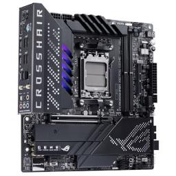 |
by Gavin Bonshor on (#62TRJ)
Over the years, multiple motherboards have captivated the market at various price points. Models like the Hero and the Formula are staples of ASUS's premium but popular ROG-themed offerings. One such series that was once the staple of ASUS's Intel models based on the micro-ATX form factor was the Gene, last seen in the days of Intel's 8th and 9th Gen Core series (2019). In what looks to be a resurrection of the Gene series for the release of AMD's Ryzen 7000 processors based on its latest 5nm Zen 4 microarchitecture, ASUS has announced that the Gene is back via the ROG Crosshair X670E Gene.Throughout the years, the ROG Gene series has been synonymous with highly premium micro-ATX offerings, and it looks as though the ASUS ROG Crosshair X670E Gene is no different this time. Some of the ROG Crosshair X670E Gene's main features include a full-length PCIe 5.0 x16 slot, one PCIe 4.0 x1 slot, and a single PCIe 4.0 x4 M.2 slot. ASUS includes another expansion slot next to the two DDR5 memory slots for an included ROG Gen-Z.2 M.2 add-in card with support for up to two PCIe 5.0 x4 M.2 drives.The ASUS ROG Crosshair X670E Gene will also feature a 16+2 phase power delivery with premium 110 A power stages, an Intel-based 2.5 GbE, and Wi-Fi 6E networking pairing, as well as support for USB 3.2 G2x2 with Quick Charge 4+ (60 W) capability. ASUS also states that it will also have rear panel USB4 support, although ASUS hasn't provided full specifications to us at this time.At the time of writing, ASUS hasn't revealed much for the ROG Crosshair X670E Gene, nor how much it is expected to cost or when it might hit retail shelves.
|
 |
by Anton Shilov on (#62P8J)
Samsung on Friday broke ground for a new semiconductor research and development complex which will design new fabrication processes for memory and logic, as well as conduct fundamental research of next-generation technologies and materials. The company plans to invest KRW 20 trillion ($15 billion) in the new R&D facility by 2028.To make more competitive logic and memory chips, companies like Samsung have to innovate across many directions, which includes new materials (for fins, for gates, for contacts, for dielectrics, just to name a few), transistor architecture, manufacturing technologies, and design of actual devices. In many cases, companies physically separate fundamental research and development of actual process technologies, but the new R&D center will conduct operations across virtually all fronts except device design.The new facility will handle advanced research on next-generation transistors and fabrication processes for memory and logic chips as well as seek for new technologies to 'overcome the limits of semiconductor scaling.' Essentially, this means researching new materials and manufacturing techniques as well as developing actual production nodes. Given that all of these R&D operations require large scale nowadays, it is not particularly surprising that it will require Samsung to invest $15 billion in the center over the next six years.Spreading fundamental research and applied development operations across different locations helps with bringing new talent onboard (e.g., people with academia background may be unwilling to relocate too far away from their current homes), but also creates discrepancy within one company as feedback from different departments gets slower. Ideally, scientists doing pathfinding and research, developers designing new production nodes, fab engineers, and device developers should work together on a site and get feedback from each other. But while Samsung's new R&D hub is not meant for this, it will still bring scientists and node developers together, which is a big deal.The new R&D center will be located at Samsung's campus near Giheung, South Korea, and will be occupy around 109,000 m (~20 football fields). To put the number into a more relevant context, Apple's corporate headquarters — Apple Park — occupies around 259,000 m and houses over 12,000 of employees that do everything from management to research to product development.The new R&D facility will work in concert with Samsung's existing R&D line in Hwaseong (which works on memory, system LSI, and foundry technologies) and the company's production complex in Pyeongtaek that can produce both DRAM (using 10nm-class technologies) and logic chips (using 5nm-class and thinner nodes). It will also be Samsung's 12 semiconductor R&D center. Meanwhile, this will be the company's first semiconductor R&D facility of this scale.Three years ago Samsung announced plans to spend KRW 133 trillion ($100 billion today, $115 billion in 2019) on semiconductor R&D by 2030. The company allocated KRW 73 trillion ($54.6 billion) on R&D operations in South Korea, so investing $15 billion in a single research and development facility aligns perfectly with this plan."Our new state-of-the-art R&D complex will become a hub for innovation where the best research talent from around the world can come and grow together," said President Kye Hyun Kyung, who also heads the Device Solutions (DS) Division. "We expect this new beginning will lay the foundation for sustainable growth of our semiconductor business."Source: Samsung
|