Breakthrough Could Lead to Amplifiers for 6G Signals

With 5G just rolling out and destined to take years to mature, it might seem odd to worry about 6G. But some engineers say that this is the perfect time to worry about it. One group, based at the University of California, Santa Barbara, has been developing a device that could be critical to efficiently pushing 6G's terahertz-frequency signals out of the antennas of future smartphones and other connected devices. They reported key aspects of the device-including an n-polar" gallium nitride high-electron mobility transistor-in two papers that recently appeared in IEEE Electron Device Letters.
Testing so far has focused on 94 gigahertz frequencies, which are at the edge of terahertz. We have just broken through records of millimeter-wave operation by factors which are just stunning," says Umesh K. Mishra, an IEEE Fellow who heads the UCSB group that published the papers. If you're in the device field, if you improve things by 20 percent people are happy. Here, we have improved things by 200 to 300 percent."
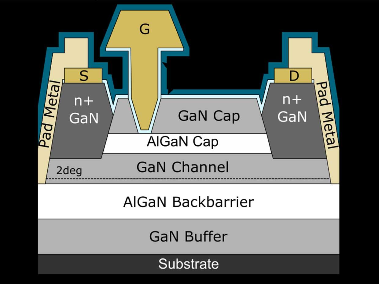
The key power amplifier technology is called a high-electron-mobility transistor (HEMT). It is formed around a junction between two materials having different bandgaps: in this case, gallium nitride and aluminum gallium nitride. At this heterojunction," gallium nitride's natural polarity causes a sheet of excess charge called a two-dimensional electron gas to collect. The presence of this charge gives the device the ability to operate at high frequencies, because the electrons are free to move quickly through it without obstruction.
Gallium nitride HEMTs are already making their mark in amplifiers, and they are a contender for 5G power amplifiers. But to efficiently amplify terahertz frequencies, the typical GaN HEMT needs to scale down in a particular way. Just as with silicon logic transistors, bringing a HEMT's gate closer to the channel through which current flows-the electron gas in this case-lets it control the flow of current using less energy, making the device more efficient. More specifically, explains Mishra, you want to maximize the ratio of the length of the gate versus the distance from the gate to the electron gas. That's usually done by reducing the amount of barrier material between the gate's metal and the rest of the device. But you can only go so far with that strategy. Eventually it will be too thin to prevent current from leaking through, therefore harming efficiency.
But Mishra says his group has come up with a better way: They stood the gallium nitride on its head.
Ordinary gallium nitride is what's called gallium-polar. That is, if you look down at the surface, the top layer of the crystal will always be gallium. But the Santa Barbara team discovered a way to make nitrogen-polar crystals, so that the top layer is always nitrogen. It might seem like a small difference, but it means that the structure that makes the sheet of charge, the heterojunction, is now upside down.
This delivers a bunch of advantages. First, the source and drain electrodes now make contact with the electron gas via a lower band-gap material (a nanometers-thin layer of GaN) rather than a higher-bandgap one (aluminum gallium nitride), lowering resistance. Second, the gas itself is better confined as the device approaches its lowest current state, because the AlGaN layer beneath acts as a barrier against scattered charge.
Devices made to take advantage of these two characteristics have already yielded record-breaking results. At 94 GHz, one device produced 8.8 Watts per millimeter at 27 percent efficiency. A similar gallium-polar device produced only about 2 W/mm at that efficiency.
 Illustration: University of California, Santa Barbara A two-dimensional electronic gas (2DEG) in the HEMT's gallium nitride channel allows for high-frequency amplification.
 But the new geometry also allows for further improvements by positioning the gate even closer to the electron gas, giving it better control. For this to work, however, the gate has to act as a low-leakage Schottky diode. Unlike ordinary p-n junction diodes, which are formed by the junction of regions of semiconductor chemically doped to have different excess charges, Schottky diodes are formed by a layer of metal, insulator, and semiconductor. The Schottky diode Mishra's team cooked up-ruthenium deposited one atomic layer at a time on top of N-polar GaN-provides a high barrier against current sneaking through it. And, unlike in other attempts at the gate diode, this one doesn't lose current through random pathways that shouldn't exist in theory but do in real life.
Schottky diodes are typically extremely difficult to get on GaN without them being leaky," says Mishra. We showed that this material combination... gave us the nearly ideal Schottky diode characteristics."
The UC Santa Barbara team hasn't yet published the results of from a HEMT made with this new diode as the gate, says Mishra. But the data so far is promising. And they plan to eventually test the new devices at even higher frequencies than before-140 GHz and 230 GHz-both firmly in the terahertz range.
< Back to IEEE Journal Watch