Insulator-Conductor Transition Points Toward Ultra-Efficient Computing

For the first time, researchers have been able to image how atoms in a computer switch move around on fast timescales while it turns on and off. This ability to peer into the atomic world may hold the key to a new kind of switch for computers that will speed up computing and reduce the energy required for computer processing.
The research team made up of scientists from the Department of Energy's SLAC National Accelerator Laboratory, Stanford University, Hewlett Packard Labs, Penn State University and Purdue University were able to capture snapshots of atomic motion in a device while it was switching. The researchers believe that the new insights this technique will generate into how switches operate will not only improve future switch technology, but will also resolve the ultimate speed and energy-consumption limits for computing devices.
Switches in computer chips control the flow of electrons. By applying an electrical charge to the switch and then removing that charge, the switch can be turned back and forth between acting as an insulator that blocks the flow of electrons to a conductor that allows the flow of electrons. This on/off switch is the basis for the "0-1" of binary computer logic.
While studying a switch made from vanadium dioxide, the researchers were able to detect with their imaging technique the existence of a short-lived transition stage between the material going from an insulator to a conductor and then back again.
"In this transient state, the structure remains the same as in the starting insulating state, but there is electronic reorganization which causes it to become metallic," explained Aditya Sood, a postdoctoral researcher at SLAC National Lab & Stanford University. "We infer this from subtle signatures in how the electron diffraction pattern changes during this electrically-driven transition."
In order to observe this transient state, the researchers had to develop a real-time imaging technology based on electron diffraction. Electron diffraction by itself has existed for many decades and is used routinely in transmission electron microscopes (TEMs). But in these previous kinds of applications, electron imaging was used just to study a material's structure in a static way, or to probe its evolution on slow timescales.
While ultrafast electron diffraction (UED) has been developed to make time-resolved measurements of atomic structure, previous implementations of this technique relied on optical pulses to impulsively excite (or "pump") materials and image the resulting atomic motions.
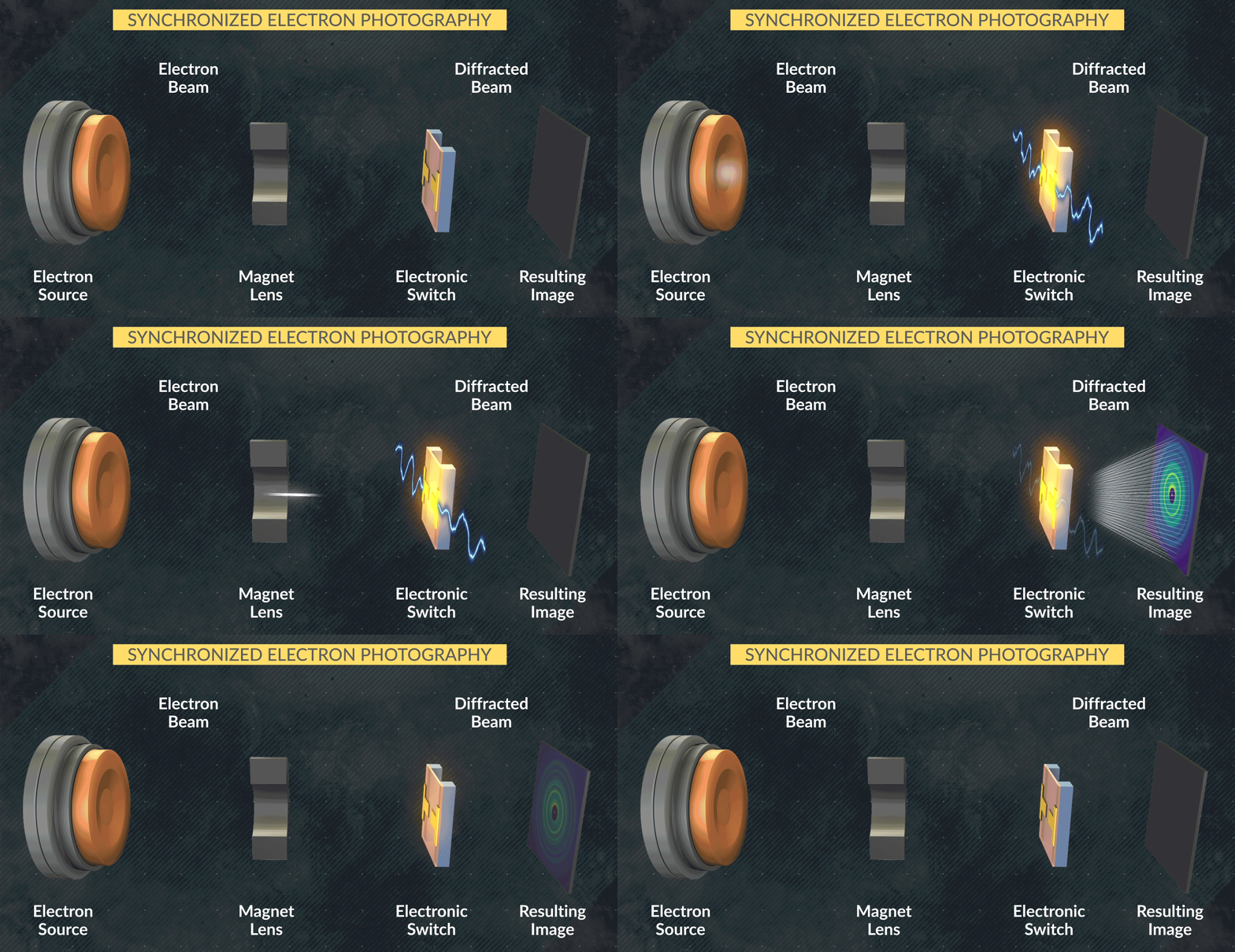
What the scientists did here for the first time in this research was create an ultrafast technique in which electrical (not optical) pulses provide the impulsive excitation. This makes it possible to electrically pulse a device, look at the ensuing atomic scale motions on fast timescales (down to nanoseconds), while simultaneously measuring current through the device.
 The team used electrical pulses, shown here in blue, to turn their custom-made switches on and off several times. They timed these electrical pulses to arrive just before the electron pulses produced by SLAC's ultrafast electron diffraction source MeV-UED, which captured the atomic motions.Greg Stewart/SLAC National Accelerator Laboratory
"We now have a direct way to correlate very fast atomic movements at the angstrom scale with electronic flow across device length scales," said Sood.
To do this, the researchers built a new apparatus that integrated an electronic device to which they could apply fast electrical bias pulses, such that each electrical bias pulse was followed by a "probing" electron pulse (which creates a diffraction pattern, telling us about where the atoms are) with a controllable time delay.
"By repeating this many times, each time changing the time delay, we could effectively construct a movie of the atomic movements during and after electrical biasing," explained Sood.
Additionally, the researchers built an electrical circuit around the device to be able to concurrently measure the current flowing through during the transient switching process. While custom-made vanadium-dioxide-based switches were fabricated for the sake of this research, Sood says that the technique could work on any kind of switch just as long as the switch is 100 nanometers or thinner to allow electrons to be transmitted through it.
"It would be interesting to see if the multi-stage, transient switching phenomenon we observe in our vanadium-dioxide-based devices is found more broadly across the solid-state device landscape," said Sood. "We are thrilled by the prospect of looking at some of the emerging memory and logic technologies, where for the first time, we can visualize ultrafast atomic motions occurring during switching."
Aaron Lindenberg, a professor in the Department of Materials Science and Engineering at Stanford and a collaborator with Sood on this work said, "More generally, this work also opens up new possibilities for using electric fields to synthesize and stabilize new materials with potentially useful functional properties."
The group's research was published in a recent issue of the journal Science.