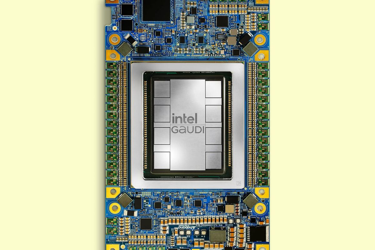
Intel’s Gaudi 3 Goes After Nvidia

Although the race to power the massive ambitions of AI companies might seem like it's all about Nvidia, there is a real competition going in AI accelerator chips. The latest example: At Intel's Vision 2024 event this week in Phoenix, Ariz., the company gave the first architectural details of its third-generation AI accelerator, Gaudi 3.
With the predecessor chip, the company had touted how close to parity its performance was to Nvidia's top chip of the time, H100, and claimed a superior ratio of price versus performance. With Gaudi 3, it's pointing to large-language-model (LLM) performance where it can claim outright superiority. But, looming in the background is Nvidia's next GPU, the Blackwell B200, expected to arrive later this year.
Gaudi Architecture EvolutionGaudi 3 doubles down on its predecessor Gaudi 2's architecture, literally in some cases. Instead of Gaudi 2's single chip, Gaudi 3 is made up of two identical silicon dies joined by a high-bandwidth connection. Each has a central region of 48 megabytes of cache memory. Surrounding that are the chip's AI workforce-four engines for matrix multiplication and 32 programmable units called tensor processor cores. All that is surrounded by connections to memory and capped with media processing and network infrastructure at one end.
Intel says that all that combines to produce double the AI compute of Gaudi 2 using 8-bit floating-point infrastructure that has emerged as key to training transformer models. It also provides a fourfold boost for computations using the BFloat 16 number format.
Intel projects a 40 percent faster training time for the GPT-3 175B large language model versus the H100 and even better results for the 7-billion and 8-billion parameter versions of Llama2.
For inferencing, the contest was much closer, according to Intel, where the new chip delivered 95 to 170 percent of the performance of H100 for two versions of Llama. Though for the Falcon 180B model, Gaudi 3 achieved as much as a fourfold advantage. Unsurprisingly, the advantage was smaller against the Nvidia H200-80 to 110 percent for Llama and 3.8x for Falcon.
Intel claims more dramatic results when measuring power efficiency, where it projects as much as 220 percent H100's value on Llama and 230 percent on Falcon.
Our customers are telling us that what they find limiting is getting enough power to the data center," says Intel's Habana Labs chief operating officer Eitan Medina.
The energy-efficiency results were best when the LLMs were tasked with delivering a longer output. Medina puts that advantage down to the Gaudi architecture's large-matrix math engines. These are 512 bits across. Other architectures use many smaller engines to perform the same calculation, but Gaudi's supersize version needs almost an order of magnitude less memory bandwidth to feed it," he says.
Gaudi 3 Versus BlackwellIt's speculation to compare accelerators before they're in hand, but there are a couple of data points to compare, particular in memory and memory bandwidth. Memory has always been important in AI, and as generative AI has taken hold and popular models reach the tens of billions of parameters in size it's become even more critical.
Both make use of high-bandwidth memory (HBM), which is a stack of DRAM memory dies atop a control chip. In high-end accelerators, it sits inside the same package as the logic silicon, surrounding it on at least two sides. Chipmakers use advanced packaging, such as Intel's EMIB silicon bridges or TSMC's chip-on-wafer-on-silicon (CoWoS), to provide a high-bandwidth path between the logic and memory.
As the chart shows, Gaudi 3 has more HBM than H100, but less than H200, B200, or AMD's MI300. It's memory bandwidth is also superior to H100's. Possibly of importance to Gaudi's price competitiveness, it uses the less expensive HBM2e versus the others' HBM3 or HBM3e, which are thought to be a significant fraction of the tens of thousands of dollars the accelerators reportedly sell for.
One more point of comparison is that Gaudi 3 is made using TSMC's N5 (sometimes called 5-nanometer) process technology. Intel has basically been a process node behind Nvidia for generations of Gaudi, so it's been stuck comparing its latest chip to one that was at least one rung higher on the Moore's Law ladder. With Gaudi 3, that part of the race is narrowing slightly. The new chip uses the same process as H100 and H200. What's more, instead of moving to 3-nm technology, the coming competitor Blackwell is done on a process called N4P. TSMC describes N4P as being in the same 5-nm family as N5 but delivering an 11 percent performance boost, 22 percent better efficiency, and 6 percent higher density.
In terms of Moore's Law, the big question is what technology the next generation of Gaudi, currently code-named Falcon Shores, will use. So far the product has relied on TSMC technology while Intel gets its foundry business up and running. But next year Intel will begin offering its 18A technology to foundry customers and will already be using 20A internally. These two nodes bring the next generation of transistor technology, nanosheets, with backside power delivery, a combination TSMC is not planning until 2026.