Screening new materials with computer vision

Boosting the performance of solar cells and other devices will require novel electronic materials that researchers are working to identify with the help of AI. Now a computer vision technique developed by MIT engineers offers a speedy way to confirm that such materials perform as expected-one of the biggest bottlenecks in the screening process.
The technique automatically analyzes images of semiconductor samples created by a robotic printer and estimates two key properties for each one: band gap (a major factor in a semiconductor's ability to convert light to electricity) and stability.
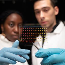
Graduate students Eunice Aissi and Alexander Siemenn, SM '21, who reported on the work with colleagues including professor of mechanical engineering Tonio Buonassisi, used the technique to analyze perovskites, materials that have great promise for solar cells but tend to degrade quickly. About 70 samples-each with a slightly different composition-were deposited on a single slide that was then scanned with a hyperspectral camera, which captures much richer visual information than a human can process. With this data, one of the algorithms they developed was able to compute the band gap for three slides of samples in a total of six minutes-a process that would take a human expert several days.
To test for stability, the team placed the slide in a chamber in which they varied conditions such as humidity, temperature, and light exposure. They photographed the samples with a standard camera every 30 seconds for two hours and used a second algorithm to estimate how they changed color over time, indicating the degree to which they degraded in the different environments. It took 20 minutes to analyze 48,000 images.
The ultimate goal is an autonomous lab, says Aissi: The whole system would allow us to give a computer a materials problem, have it predict potential compounds, and then run 24-7 making and characterizing those predicted materials until it arrives at the desired solution."