X-Ray Tech Lays Chip Secrets Bare
Scientists and engineers in Switzerland and California have come up with a technique that can reveal the 3D design of a modern microprocessor without destroying it.
Typically today, such reverse engineering is a time-consuming process that involves painstakingly removing each of a chip's many nanometers-thick interconnect layers and mapping them using a hierarchy of different imaging techniques, from optical microscopy for the larger features to electron microscopy for the tiniest features.
The inventors of the new technique, called ptychographic X-ray laminography, say it could be used by integrated circuit designers to verify that manufactured chips match their designs, or by government agencies concerned about "kill switches" or hardware trojans that could have secretly been added to ICs they depend on.
"It's the only approach to non-destructive reverse engineering of electronic chips-[and] not just reverse engineering but assurance that chips are manufactured according to design," says Anthony F. J. Levi, professor of electrical and computer engineering at University of Southern California, who led the California side of the team. "You can identify the foundry, aspects of the design, who did the design. It's like a fingerprint."
The new technique is an improvement on technology unveiled by the same team in 2017 called ptychographic computed tomography. That process used a coherent beam of X-rays from a synchrotron to illuminate a 10-micrometer pillar that had been cut away from the rest of the chip. The team then recorded how the X-rays diffract and scatter from the pillar at a variety of angles and computed what the internal structures must be in order to create that pattern.
With the new technique, "the goal was obviously to avoid having to do any cutting at all," explains Gabriel Aeppli, head of the photonic science division at the Paul Scherrer Institute (PSI) in Switzerland and professor of physics at the Swiss Federal Institutes of Technology in Zi1/4rich and Lausanne, who led the research. "A modern chip with a billion transistors is a bigger footprint than 10 microns." The group wanted a single technology that would allow them to image a whole chip and also zoom in on points of interest.
The prior technique needed the pillar, because trying to see through a whole chip, edge-on, absorbs too many of the X-rays to produce a useful diffraction pattern. But shooting the X-rays through the chip at an angle creates a small enough cross-section. However, it also produces a gap in the information. Some of that information can be regained by making some assumptions about what you're looking at, explains Aeppli. For example, we know that real interconnects can't have certain shapes.
Finding the right angle for the X-rays-which turned out to be 61 degrees-was a matter of balancing absorption and information loss, says Aeppli.
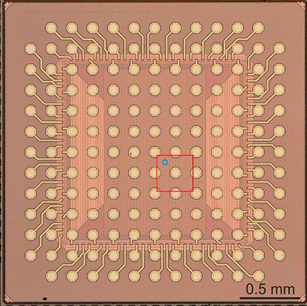
 Image: Paul Scherrer Institute The new technique was used to examine a chip made using 16 nanometer process technology. The scientists zoomed in on first the red square and then the blue circle to find progressively smaller features.
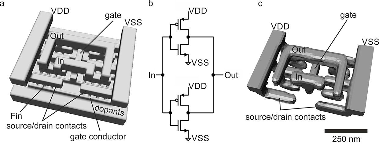
 In the new technique, the bare chip is polished down to a thickness of 20 micrometers and then placed on a scanning stage at a 61-degree tilt. The stage then rotates the chip as the X-ray beam is focused on it. A photon-counting camera receives the resulting diffraction pattern. Using the technique in low-resolution mode, the team scanned a 300-by-300-micrometer area in 30 hours. They then used it to zoom in on a 40-micrometer-diameter section to produce a 3D image with 18.9-nanometer resolution, requiring another 60 hours. Using the high-resolution mode, the researchers could identify the parts of an individual inverter circuit in a chip made using 16-nanometer node technology.
This first laminography microscope engineered by PSI's Mirko Holler, can image a maximum of 12 by 12 millimeters-easily accommodating many chips, such as the iPhone processor Apple A12, but not large enough for an entire Nvidia Volta GPU. Though the group tested the technique on a chip made using a 16-nanometer process technology, it will be able to comfortably handle those made using the new 7-nanometer process technology, where the minimum distance between metal lines is around 35 to 40 nanometers.
Future versions of the laminography technique could reach a resolution of just 2 nanometers or reduce the time for a low-resolution inspection of that 300-by-300-micrometer segment to less than an hour, the researchers say.
Those improvements will come from a new generation of synchrotron light sources. The synchrotron at PSI is considered a 3rd generation machine. But 4th generation machines are already starting up, such as Sweden's MAX IV. With a higher flux of X-ray photons flowing through the chip, the system can collect more usable data per unit of time, leading to higher resolution and faster processing. "We're looking at improvements of 1,000 to 10,000 over the next five or six years in terms of the pixels we're collecting per unit [of] time," says Aeppli.
 Images: Paul Scherrer Institute Ptychographic X-ray laminography could reveal the metal parts of an inverter [right]. Showing a good match for the circuit [middle, left].
 Ptychographic X-ray laminography can be further sped up by starting with more information about the chip. Knowing the design rules ahead of time allows the system to come to a conclusion about what it's seeing with fewer photons. In fact, Aeppli suspects one of the main uses of the technology will be to look for deviations from the design that could be indicative of manufacturing errors or something more sinister.
"Looking for deviation from design is an easier problem than reverse engineering the entire design," he says. The team is seeing "a lot of interest from the [United States] on the national security side."
However, Aeppli expects chipmakers to use the laminography technique, as well. "Every region that has major chip foundries nearby has some national lab with a synchrotron," he points out.
Aeppli, Levi, and their teams reported the technique this week in Nature Electronics.