Intel: Back on Top by 2025?

Intel has spent the last few years dealing with criticism that it had lost its lead against rivals in the race to put ever more and better performing transistors on each square millimeter of silicon. This week, Intel unveiled a roadmap that company executives say will put them at the head of the pack by 2025.
Acknowledging that the naming convention for new semiconductor manufacturing process technologies has become meaningless, Intel will stop using "nanometer" in its new node names after the 10-nanometer node, which is in high volume production now. Intel's 10-nm technology is a good illustration of the need for a name change, because the process appears to make transistor features on par with TSMC's and Samsung's 7-nm technology.
Its newest node, previously called Enhanced SuperFin, Intel has rechristened Intel 7. That technology has entered volume production, and it offers a 10-15 percent performance per watt improvement. Basically, that means a 10-15 percent faster transistor at a fixed power or 10-15 percent better power efficiency at a fixed operating frequency, or something in between. Intel 7 takes advantage of an improved version of the FinFET transistor.
In FinFETs, the transistor channel, through which current flows, is a vertical fin-shaped protrusion surrounded on three sides by the transistor gate. It's been the leading-edge configuration of the device since 2011. Intel introduced what it calls SuperFin with the 10-nm node.The next stage, Intel 4, is what the company used to call 7-nanometers. It sticks with the SuperFin, gains 20 percent performance per watt over Intel 7. The process makes more use of extreme-ultraviolet lithography, the most advanced chip-making tech, as well. Intel began making its Meteor Lake processor using the process for one client in the second quarter of 2022, and it will use it for the Granite Rapids data center chip, as well. (This stage of production is often called "risk" production, because initial customers are taking a risk that the new manufacturing process will work for their designs.)
Intel 3 will follow in the second half of 2023, using even more EUV to reduce logic cell area. It sticks with the FinFET structure, but through reduced resistance in the vertical connections to the transistor and a greater ability to drive current through the transistor, it manages an 18 percent performance per watt gain over Intel 4.
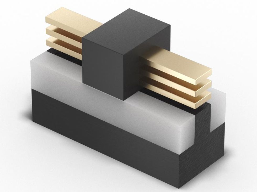
The final step the company detailed was Intel 20A, set to ramp up to volume production in 2024. The 'A' refers to the Angstrom, according to Intel, an apparent nod to the idea that the node name system has run out of nanometers. It's with Intel 20A that things get really interesting. With 20A, Intel says it will abandon the trusty FinFET for what it's calling RibbonFET but others call nanosheets. With nanosheets, the transistor channel forms in stack of sheets of semiconductor. Unlike with FinFETs, where the gate covers the channel region on three sides, the nanosheets are completely surrounded by the gate, improving the electrostatic control of the transistor, among other benefits.
Samsung's 3-nanometer technology will be based on nanosheets, which that company calls multichannel bridge FETs. It's set to begin manufacturing in 2022. Like Intel, TSMC is delaying the move away from FinFETs to a later node.
 Intel's new RibbonFET technology, the company's implementation of a gate-all-around transistor. Intel
Perhaps just as essential as the change in transistor architecture is the what Intel is calling the PowerVia. It is essential-what Imec and Arm have been calling back-side power delivery with buried power rails. In that scheme, all the interconnects that deal with delivering power rather than data, are moved beneath the transistors. This has two effects. First, it greatly reduces resistance in the power delivery network, so there's less of a voltage drop from the power source to the transistors themselves. And second, it leaves more room above the transistors for data-carrying interconnects, potentially shrinking the size of logic cells.
The combination of RibbonFET and PowerVia "will be another watershed moment in process technology," says Ann Kelleher, senior vice president and general manager of Technology Development at Intel. The company is developing 20A's successor as well, to be called 18A. It will include refinements of the RibbonFET for better performance. It may be helped along by new lithography technology under development at ASML called high numerical aperture EUV. Intel says it will be the first chip company to deploy a High NA system.
Intel Introduces New RibbonFET and PowerVia Technologies
To help keep it on top and boost its foundry business as well, Intel is also counting on advances in its advanced packaging technologies. These will expand an already-begun move toward building systems out of multiple smaller dies called chiplets instead of a single large piece of silicon. This allows different circuits and logic blocks to be built using the most appropriate process technology. For example, processor tiles can be constructed using the most advanced node, while an older, more economic node is employed to build the less demanding systems.
 Intel
Intel
The company plans to boost the density of connections for its EMIB technology, which is used to link two silicon dies horizontally in the same package. In 2023 it will also introduce two new 3D chip stacking technologies Foveros Omni and Foveros Direct. Omni increases the flexibility of Foveros, the company says. Direct increases the density of interconnects in the 3D stack by an order of magnitude.