Samsung Speeds AI With Processing in Memory

One of the long-standing limiters in big AI neural nets is the time and energy needed to send huge amounts of data between the processor and memory. But what if the processor were in the memory? That's the solution memory-giant Samsung detailed this week at IEEE Hot Chips. Earlier this year, the company developed compute cores inside its high-bandwidth memory (HBM), the kind of dynamic random-access memory (DRAM) that surrounds some top AI accelerator chips. This week Samsung detailed its first tests of the processor-in-memory (PIM) tech in a customer's system-the Xilinx Virtex Ultrascale+ (Alveo) AI accelerator-delivering a nearly 2.5-fold performance gain as well as more than a 62 percent cut in energy consumption, for a speech recognition neural net. Samsung, which is the largest maker of DRAM in the world, is now also developing the HBM-PIM technology for low-power memory used in mobile devices.
"New and emerging AI demand more and more memory bandwidth as [neural network] models get larger and more complex," says Nam Sung Kim, senior vice president of Samsung's memory business unit and an IEEE Fellow. "Because of the limited number of [printed circuit board] wires to the chip packages, along with the power and some constraints of those chip packages, it's getting really hard and expensive to keep increasing the bandwidth."
Neural networks are so large that the data defining them must often be loaded onto GPUs and other processors in portions. Designers try to speed the process up by putting the DRAM inside the package with the processor chip, or experimentally at least, building memory in the layers of interconnect above the logic transistors. The extreme solution is to make the processor so big that it can contain all of the data without any need for external memory. But the biggest neural networks will eventually outstrip even this scheme.
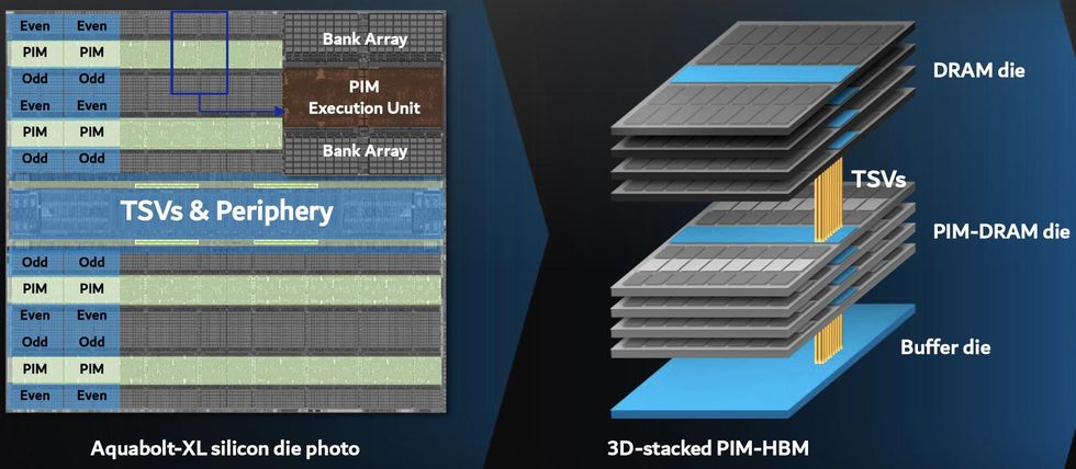
By doing some of the compute in the DRAM, engineers reason, the total volume of data that needs to go to the processor decreases, effectively speeding up the neural network and saving the power needed to transport data. Samsung developed HBM-PIM as a drop-in-replacement for its existing HBM2 product, a multi-gigabit stack of DRAM chips linked together vertically by interconnects called through-silicon vias. In the new product, called Aquabolt XL, the bottom four of 8 memory chips are replaced with chips containing both DRAM and compute cores.
 Increasing the number of connections between DRAM and the CPU are not an option, but adding logic to DRAM reduces the amount of data that has to move between the CPU and DRAM.Samsung
According to Kim, the HBM-PIM does best for tasks that are limited by memory rather than limited by compute resources. These include speech recognition, machine translation, and recommender systems. "It's not designed to compete with the AI accelerator but to complement it," says Kim. The processing part of the PIM is deliberately limited. It executes only nine instructions, which are mostly performed by 16-bit floating point multiplier and adder units. (Much of the math of neural networks consists of a combination multiplication and addition.)
Adding PIM means the DRAM chip consumes 5.4 percent more energy than it would otherwise. But as part of a system it reduces the average power during execution and cuts the execution time, so the power consumed by the system as a whole falls. For the Xilinx integration, system power consumption fell 62 percent when operating the RNN-Transducer speech recognition neural network.
Samsung is also adapting the technology to the low-power version of DRAM used in mobile devices, LPDDR5. A system-level simulation using that technology about doubled energy efficiency and performance (how quickly it does its job), for common language-related neural nets while approximately doubling performance. Gains were more modest for computer vision, around 10 percent.
 HBM-PIM adds processing to the bottom four DRAM chips in a stack of eight. As in ordinary HBM, the chips are linked vertically with through-silicon vias (TSVs).Samsung
A big step in getting PIM adopted in AI systems is making it easy to use. From the standpoint of a system layout, Aquabolt XL is identical to ordinary HBM2. And Samsung is working with JEDEC on a standard. But with AI, software can make or break a product. Kim explains that the chips have a software stack that works using the widely used neural network frameworks Pytorch and TensorFlow without changes to the source code. It can operate either in a mode where it automatically sends "PIM-friendly" code to the DRAM or one where the programmer explicitly says which code to execute there.
Samsung expects to have the HBM-PIM standard worked out in early 2022. It is providing engineering samples to partners now.
Many other companies and researchers are chasing processing-in-memory of one sort or another. For example, researchers at Korea Advanced Institute of Science and Technology (KAIST) proposed a PIM-HBM scheme that put all the computing in a die at the bottom of the HBM stack, Renesas reported a Flash memory-based architecture, and IBM created one based on phase-change memory.