How the First Transistor Worked
The vacuum-tube triode wasn't quite 20 years old when physicists began trying to create its successor, and the stakes were huge. Not only had the triode made long-distance telephony and movie sound possible, it was driving the entire enterprise of commercial radio, an industry worth more than a billion dollars in 1929. But vacuum tubes were power-hungry and fragile. If a more rugged, reliable, and efficient alternative to the triode could be found, the rewards would be immense.
The goal was a three-terminal device made out of semiconductors that would accept a low-current signal into an input terminal and use it to control the flow of a larger current flowing between two other terminals, thereby amplifying the original signal. The underlying principle of such a device would be something called the field effect-the ability of electric fields to modulate the electrical conductivity of semiconductor materials. The field effect was already well known in those days, thanks to diodes and related research on semiconductors.
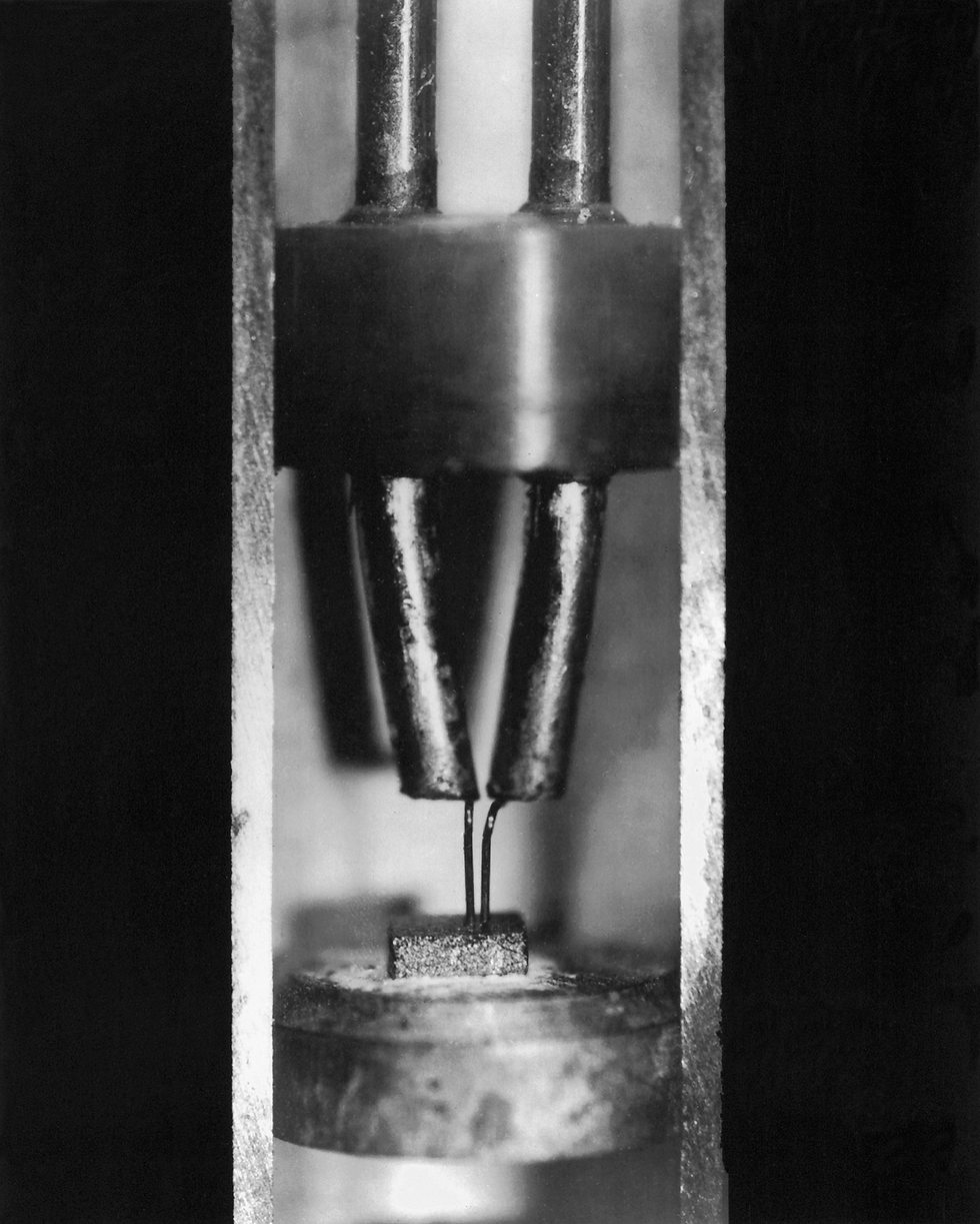 In the cutaway photo of a point-contact, two thin conductors are visible; these connect to the points that make contact with a tiny slab of germanium. One of these points is the emitter and the other is the collector. A third contact, the base, is attached to the reverse side of the germanium.AT&T ARCHIVES AND HISTORY CENTER
But building such a device had proved an insurmountable challenge to some of the world's top physicists for more than two decades. Patents for transistor-like devices had been filed starting in 1925, but the first recorded instance of a working transistor was the legendary point-contact device built at AT&T Bell Telephone Laboratories in the fall of 1947.
Though the point-contact transistor was the most important invention of the 20th century, there exists, surprisingly, no clear, complete, and authoritative account of how the thing actually worked. Modern, more robust junction and planar transistors rely on the physics in the bulk of a semiconductor, rather than the surface effects exploited in the first transistor. And relatively little attention has been paid to this gap in scholarship.
It was an ungainly looking assemblage of germanium, plastic, and gold foil, all topped by a squiggly spring. Its inventors were a soft-spoken Midwestern theoretician, John Bardeen, and a voluble and somewhat volatile" experimentalist, Walter Brattain. Both were working under William Shockley, a relationship that would later prove contentious. In November 1947, Bardeen and Brattain were stymied by a simple problem. In the germanium semiconductor they were using, a surface layer of electrons seemed to be blocking an applied electric field, preventing it from penetrating the semiconductor and modulating the flow of current. No modulation, no signal amplification.
Sometime late in 1947 they hit on a solution. It featured two pieces of barely separated gold foil gently pushed by that squiggly spring into the surface of a small slab of germanium.
Textbooks and popular accounts alike tend to ignore the mechanism of the point-contact transistor in favor of explaining how its more recent descendants operate. Indeed, the current edition of that bible of undergraduate EEs, The Art of Electronics by Horowitz and Hill, makes no mention of the point-contact transistor at all, glossing over its existence by erroneously stating that the junction transistor was a Nobel Prize-winning invention in 1947." But the transistor that was invented in 1947 was the point-contact; the junction transistor was invented by Shockley in 1948.
So it seems appropriate somehow that the most comprehensive explanation of the point-contact transistor is contained within John Bardeen's lecture for that Nobel Prize, in 1956. Even so, reading it gives you the sense that a few fine details probably eluded even the inventors themselves. A lot of people were confused by the point-contact transistor," says Thomas Misa, former director of the Charles Babbage Institute for the History of Science and Technology, at the University of Minnesota.
Textbooks and popular accounts alike tend to ignore the mechanism of the point-contact transistor in favor of explaining how its more recent descendants operate.
A year after Bardeen's lecture, R. D. Middlebrook, a professor of electrical engineering at Caltech who would go on to do pioneering work in power electronics, wrote: Because of the three-dimensional nature of the device, theoretical analysis is difficult and the internal operation is, in fact, not yet completely understood."
Nevertheless, and with the benefit of 75 years of semiconductor theory, here we go. The point-contact transistor was built around a thumb-size slab of n-type germanium, which has an excess of negatively charged electrons. This slab was treated to produce a very thin surface layer that was p-type, meaning it had an excess of positive charges. These positive charges are known as holes. They are actually localized deficiencies of electrons that move among the atoms of the semiconductor very much as a real particle would. An electrically grounded electrode was attached to the bottom of this slab, creating the base of the transistor. The two strips of gold foil touching the surface formed two more electrodes, known as the emitter and the collector.
That's the setup. In operation, a small positive voltage-just a fraction of a volt-is applied to the emitter, while a much larger negative voltage-4 to 40 volts-is applied to the collector, all with reference to the grounded base. The interface between the p-type layer and the n-type slab created a junction just like the one found in a diode: Essentially, the junction is a barrier that allows current to flow easily in only one direction, toward lower voltage. So current could flow from the positive emitter across the barrier, while no current could flow across that barrier into the collector.
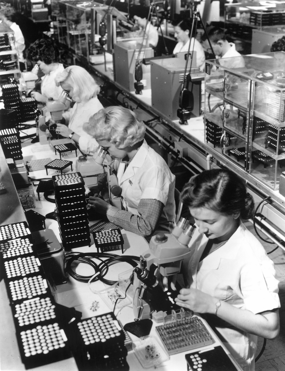 The Western Electric Type-2 point-contact transistor was the first transistor to be manufactured in large quantities, in 1951, at Western Electric's plant in Allentown, Pa. By 1960, when this photo was taken, the plant had switched to producing junction transistors.AT&T ARCHIVES AND HISTORY CENTER
Now, let's look at what happens down among the atoms. First, we'll disconnect the collector and see what happens around the emitter without it. The emitter injects positive charges-holes-into the p-type layer, and they begin moving toward the base. But they don't make a beeline toward it. The thin layer forces them to spread out laterally for some distance before passing through the barrier into the n-type slab. Think about slowly pouring a small amount of fine powder onto the surface of water. The powder eventually sinks, but first it spreads out in a rough circle.
Now we connect the collector. Even though it can't draw current by itself through the barrier of the p-n junction, its large negative voltage and pointed shape do result in a concentrated electric field that penetrates the germanium. Because the collector is so close to the emitter, and is also negatively charged, it begins sucking up many of the holes that are spreading out from the emitter. This charge flow results in a concentration of holes near the p-n barrier underneath the collector. This concentration effectively lowers the height" of the barrier that would otherwise prevent current from flowing between the collector and the base. With the barrier lowered, current starts flowing from the base into the collector-much more current than what the emitter is putting into the transistor.
The amount of current depends on the height of the barrier. Small decreases or increases in the emitter's voltage cause the barrier to fluctuate up and down, respectively. Thus very small changes in the the emitter current control very large changes at the collector, so voila! Amplification. (EEs will notice that the functions of base and emitter are reversed compared with those in later transistors, where the base, not the emitter, controls the response of the transistor.)
Ungainly and fragile though it was, it was a semiconductor amplifier, and its progeny would change the world. And its inventors knew it. The fateful day was 16 December 1947, when Brattain hit on the idea of using a plastic triangle belted by a strip of gold foil, with that tiny slit separating the emitter and collector contacts. This configuration gave reliable power gain, and the duo knew then that they had succeeded. In his carpool home that night, Brattain told his companions he'd just done the most important experiment that I'd ever do in my life" and swore them to secrecy. The taciturn Bardeen, too, couldn't resist sharing the news. As his wife, Jane, prepared dinner that night, he reportedly said, simply, We discovered something today." With their children scampering around the kitchen, she responded, That's nice, dear."
It was a transistor, at last, but it was pretty rickety. The inventors later hit on the idea of electrically forming the collector by passing large currents through it during the transistor's manufacturing. This technique enabled them to get somewhat larger current flows that weren't so tightly confined within the surface layer. The electrical forming was a bit hit-or-miss, though. They would just throw out the ones that didn't work," Misa notes.
Nevertheless, point-contact transistors went into production at many companies, under license to AT&T, and, in 1951, at AT&T's own manufacturing arm, Western Electric. They were used in hearing aids, oscillators, telephone-routing gear, in an experimental TV receiver built at RCA, and in the Tradic, the first airborne digital computer, among other systems. In fact, point-contact transistors remained in production until 1966, in part due to their superior speed compared with the alternatives.
The fateful day was 16 December 1947, when Brattain hit on the idea of using a plastic triangle belted by a strip of gold foil...
The Bell Labs group wasn't alone in its successful pursuit of a transistor. In Aulnay-sous-Bois, a suburb northeast of Paris, two German physicists, Herbert Matare and Heinrich Welker, were also trying to build a three-terminal semiconductor amplifier. Working for a French subsidiary of Westinghouse, they were following up on very intriguing observations Matare had made while developing germanium and silicon rectifiers for the German military in 1944. The two succeeded in creating a reliable point-contact transistor in June 1948.
They were astounded, a week or so later, when Bell Labs finally revealed the news of its own transistor, at a press conference on 30 June 1948. Though they were developed completely independently, and in secret, the two devices were more or less identical.
Here the story of the transistor takes a weird turn, breathtaking in its brilliance and also disturbing in its details. Bardeen's and Brattain's boss, William Shockley, was furious that his name was not included with Bardeen's and Brattain's on the original patent application for the transistor. He was convinced that Bardeen and Brattain had merely spun his theories about using fields in semiconductors into their working device, and had failed to give him sufficient credit. Yet in 1945, Shockley had built a transistor based on those very theories, and it hadn't worked.
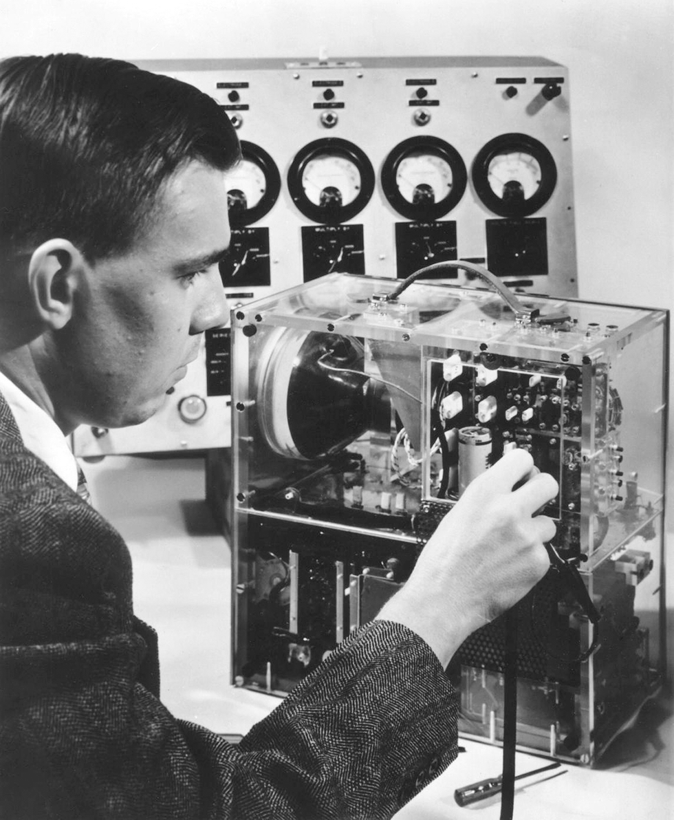 In 1953, RCA engineer Gerald Herzog led a team that designed and built the first "all-transistor" television (although, yes, it had a cathode-ray tube). The team used point-contact transistors produced by RCA under a license from Bell Labs. TRANSISTOR MUSEUM JERRY HERZOG ORAL HISTORY
At the end of December, barely two weeks after the initial success of the point-contact transistor, Shockley traveled to Chicago for the annual meeting of the American Physical Society. On New Year's Eve, holed up in his hotel room and fueled by a potent mix of jealousy and indignation, he began designing a transistor of his own. In three days he scribbled some 30 pages of notes. By the end of the month, he had the basic design for what would become known as the bipolar junction transistor, or BJT, which would eventually supersede the point-contact transistor and reign as the dominant transistor until the late 1970s.
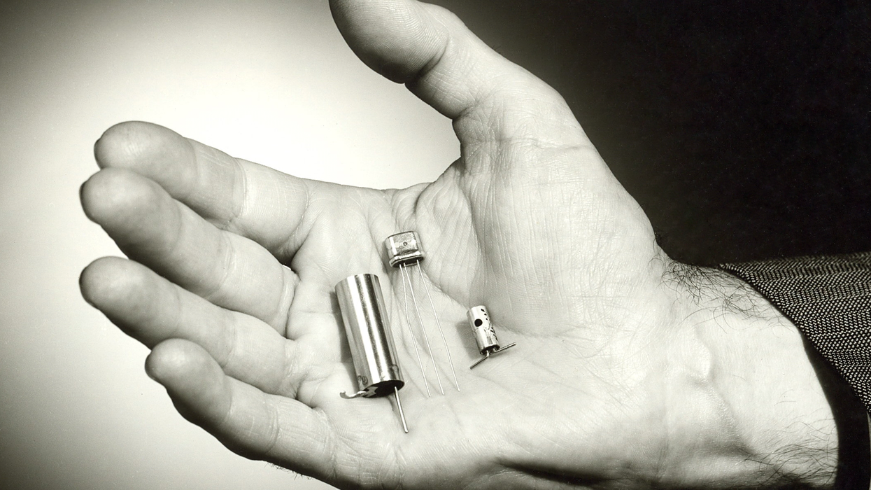
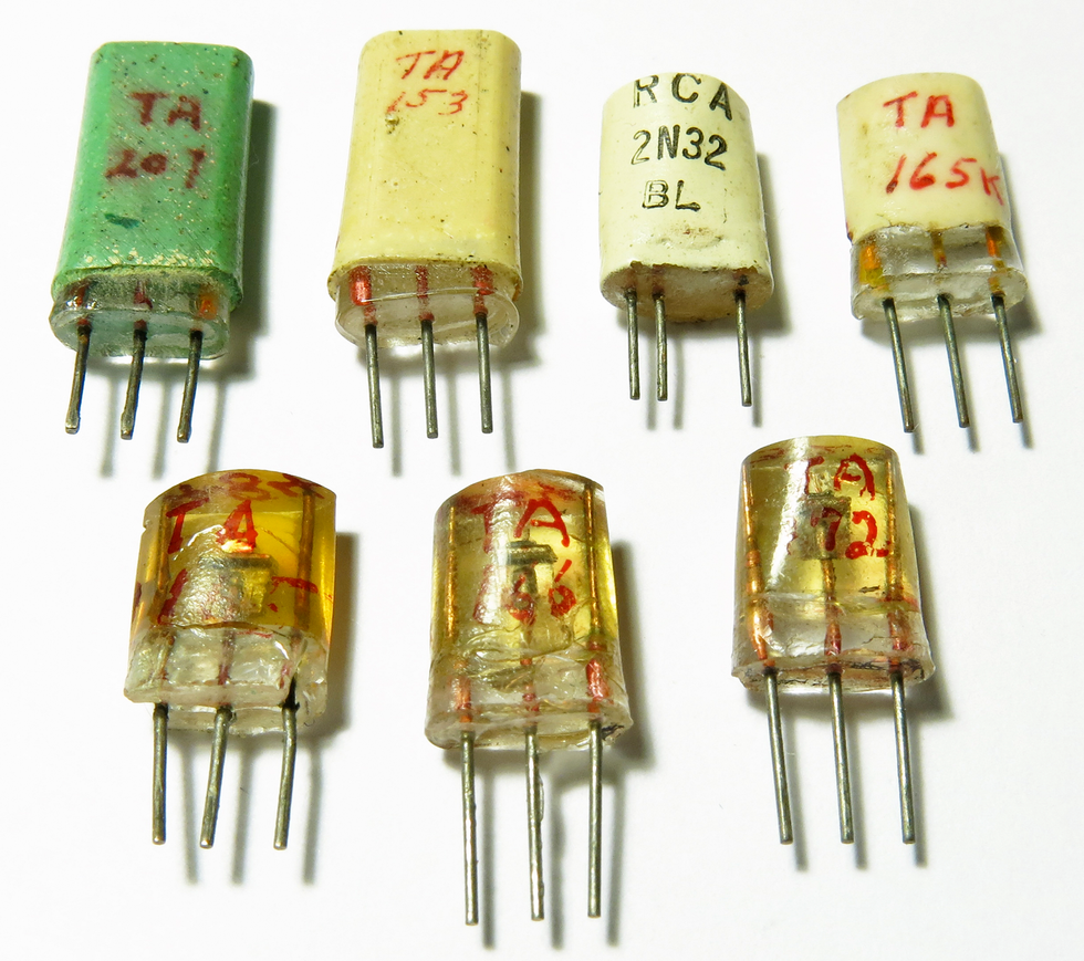 With insights gleaned from the Bell Labs work, RCA began developing its own point-contact transistors in 1948. The group included the seven shown here-four of which were used in RCA's experimental, 22-transistor television set built in 1953. These four were the TA153 [top row, second from left], the TA165 [top, far right], the TA156 [bottom row, middle] and the TA172 [bottom, right].TRANSISTOR MUSEUM JONATHAN HOPPE COLLECTION
The BJT was based on Shockley's conviction that charges could, and should, flow through the bulk semiconductors rather than through a thin layer on their surface. The device consisted of three semiconductor layers, like a sandwich: an emitter, a base in the middle, and a collector. They were alternately doped, so there were two versions: n-type/p-type/n-type, called NPN," and p-type/n-type/p-type, called PNP."
The BJT relies on essentially the same principles as the point-contact, but it uses two p-n junctions instead of one. When used as an amplifier, a positive voltage applied to the base allows a small current to flow between it and the emitter, which in turn controls a large current between the collector and emitter.
Consider an NPN device. The base is p-type, so it has excess holes. But it is very thin and lightly doped, so there are relatively few holes. A tiny fraction of the electrons flowing in combines with these holes and are removed from circulation, while the vast majority (more than 97 percent) of electrons keep flowing through the thin base and into the collector, setting up a strong current flow.
But those few electrons that do combine with holes must be drained from the base in order to maintain the p-type nature of the base and the strong flow of current through it. That removal of the trapped" electrons is accomplished by a relatively small flow of current through the base. That trickle of current enables the much stronger flow of current into the collector, and then out of the collector and into the collector circuit. So, in effect, the small base current is controlling the larger collector circuit.
Electric fields come into play, but they do not modulate the current flow, which the early theoreticians thought would have to happen for such a device to function. Here's the gist: Both of the p-n junctions in a BJT are straddled by depletion regions, in which electrons and holes combine and there are relatively few mobile charge carriers. Voltage applied across the junctions sets up electric fields at each, which push charges across those regions. These fields enable electrons to flow all the way from the emitter, across the base, and into the collector.
In the BJT, the applied electric fields affect the carrier density, but because that effect is exponential, it only takes a little bit to create a lot of diffusion current," explains Ioannis John" Kymissis, chair of the department of electrical engineering at Columbia University.
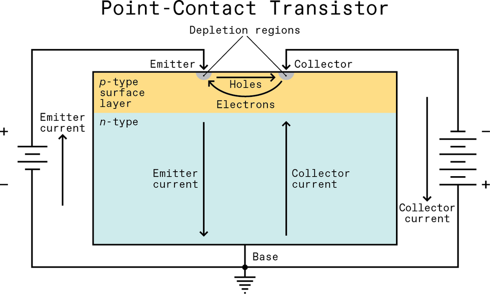 The very first transistors were a type known as point contact, because they relied on metal contacts touching the surface of a semiconductor. They ramped up output current-labeled Collector current" in the top diagram-by using an applied voltage to overcome a barrier to charge flow. Small changes to the input, or emitter," current modulate this barrier, thus controlling the output current.
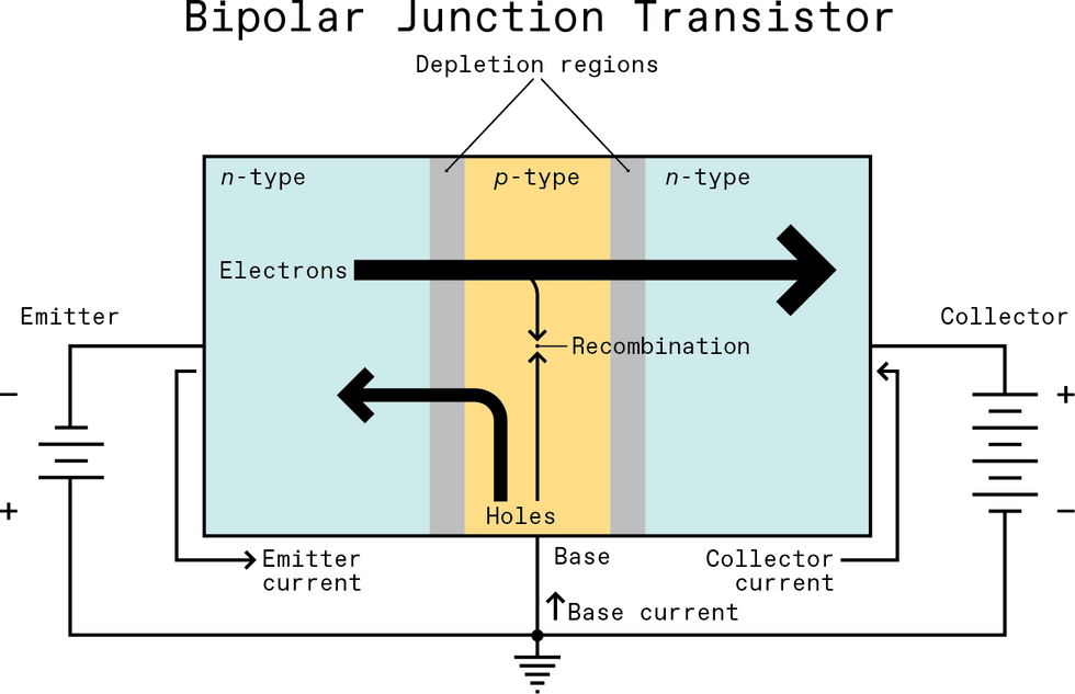 The bipolar junction transistor accomplishes amplification using much the same principles but with two semiconductor interfaces, or junctions, rather than one. As with the point-contact transistor, an applied voltage overcomes a barrier and enables current flow that is modulated by a smaller input current. In particular, the semiconductor junctions are straddled by depletion regions, across which the charge carriers diffuse under the influence of an electric field.Chris Philpot
The BJT was more rugged and reliable than the point-contact transistor, and those features primed it for greatness. But it took a while for that to become obvious. The BJT was the technology used to make integrated circuits, from the first ones in the early 1960s all the way until the late 1970s, when metal-oxide-semiconductor field-effect transistors (MOSFETs) took over. In fact, it was these field-effect transistors, first the junction field-effect transistor and then MOSFETs, that finally realized the decades-old dream of a three-terminal semiconductor device whose operation was based on the field effect-Shockley's original ambition.
Such a glorious future could scarcely be imagined in the early 1950s, when AT&T and others were struggling to come up with practical and efficient ways to manufacture the new BJTs. Shockley himself went on to literally put the silicon into Silicon Valley. He moved to Palo Alto and in 1956 founded a company that led the switch from germanium to silicon as the electronic semiconductor of choice. Employees from his company would go on to found Fairchild Semiconductor, and then Intel.
Later in his life, after losing his company because of his terrible management, he became a professor at Stanford and began promulgating ungrounded and unhinged theories about race, genetics, and intelligence. In 1951 Bardeen left Bell Labs to become a professor at the University of Illinois at Urbana-Champaign, where he won a second Nobel Prize for physics, for a theory of superconductivity. (He is the only person to have won two Nobel Prizes in physics.) Brattain stayed at Bell Labs until 1967, when he joined the faculty at Whitman College, in Walla Walla, Wash.
Shockley died a largely friendless pariah in 1989. But his transistor would change the world, though it was still not clear as late as 1953 that the BJT would be the future. In an interview that year, Donald G. Fink, who would go on to help establish the IEEE a decade later, mused, Is it a pimpled adolescent, now awkward, but promising future vigor? Or has it arrived at maturity, full of languor, surrounded by disappointments?"
It was the former, and all of our lives are so much the better because of it.
This article appears in the December 2022 print issue as The First Transistor and How it Worked ."