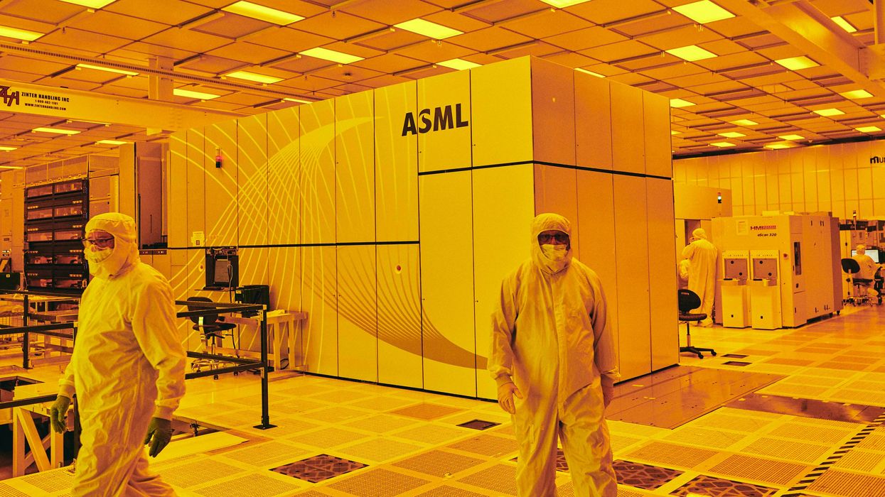
The Semiconductor Industry’s Most Important Tool Goes Green

In the complex quest to keep increasing the density of transistors, extreme ultraviolet (EUV) lithography is the most critical tool. Costing more than US $100 million, these trailer-size systems bounce near x-ray wavelength light off a complex cascade of mirrors and onto silicon wafers to create patterns with nanometer-scale precision. Because the system's 13.5-nanometer light is absorbed by air, the whole mechanism exists in a vacuum. Well, almost.
There are enough contaminants in the system and the process that the machine needs several fine flows of hydrogen to sweep away anything that could muck up its delicate optics. These flows blow through about 600 liters of the gas per minute, with that amount likely to rise in the future.
Today, the resulting contaminated hydrogen is usually burned to form water. So the supply must constantly be replenished with new hydrogen. The problem is that most hydrogen is not made using green energy-it's made by processing natural gas with steam, releasing carbon dioxide both in the chemical process and from whatever energy source produced the steam. In an effort to lower EUV's environmental footprint and its cost of ownership, engineers at Edwards, an England-based vacuum systems firm, came up with a way to recycle as much as 80 percent of the gas.
It's similar to a fuel cell, in reverse."-Anthony Keen, Edwards Vacuum
Wanting to recover the hydrogen is a bit of a no-brainer," says Anthony Keen, a technology manager at Edwards. You could turn it into electricity, which is a nice, green, circular thing. But you'd still be consuming 100 percent of your resource. To clean up the hydrogen and send it back to the machine is actually the most effective."
Hydrogen flows in several parts of the EUV machine. For example, a curtainlike flow acts as a barrier between most of the optics and the silicon wafer, which at that stage is coated in photo-active chemicals that could contaminate the chamber. But the bulk of the hydrogen, and the focus of Edwards's hydrogen recovery system, is used in the EUV light source. Here, kilowatt-class lasers zap droplets of molten tin in midflight, blasting them into plasma that glows with EUV. The hydrogen flow keeps vaporized tin from mucking up the system's optics. It's also important in carrying away the scorching heat of the plasma generation.
The semiconductor industry could reach 3 percent of global emissions by 2040.
Edwards's hydrogen recovery system is similar to a fuel cell, in reverse," says Keen. After mixing the gas with a bit of moisture and nitrogen, the hydrogen is ionized, and an electric field forces the resulting ions through a proton-exchange membrane. On the other side of the membrane, the protons recombine with electrons to form pure hydrogen. And a final purification step removes any water that migrated through the membrane. All the contaminants remain on the other side of the cell, where they can be collected and disposed of.
As part of Imec's Sustainable Semiconductor Technologies and Systems program, Edwards and Imec tested a recovery system with 80 electrochemical stacks capable of handling up to 750 standard liters per minute on Imec's 300-millimeter silicon pilot line. The tests showed that the system recovered 70 to 80 percent of the hydrogen and resulted in a net reduction in energy consumption.
Having proven what it can do, Edwards must now make the case to top chipmakers, such as Intel, Samsung, and TSMC. Chipmakers and the suppliers of chipmaking tools are striving to reduce integrated circuit production's carbon footprint, which Imec estimates could reach 3 percent of global emissions by 2040.