SK hynix to invest $712.5 billion in South Korean operations — Cheongju NAND expansion, Yongin Semiconductor Cluster for DRAM detailed
SK hynix this week announced that it would invest an additional KRW 100 trillion ($64 billion) in its Cheongju campus to expand production of 3D NAND and HBM packaging at the site. Given the vast investment, expect the company to add some massive production capacity, but unfortunately that production capacity is going to kick in only several years down the road. But that investment pales in front of the company's plan to invest $712.5 billion in its South Korean operations.
The massive KRW 100 trillion ($64 billion) in its Cheongju campus investment is only a part of SK hynix's grand plan to invest KRW 1.1 trillion ($712.5 billion) in a variety of projects in South Korea. In particular, the company intends to invest KRW 400 trillion ($259.5 billion) in its all-new Southwestern semiconductor cluster as well as KRW 600 trillion ($389.3 billion) in its Yongin site. While the Cheongju investment is considerably lower than investments in other campuses, it is the only project that is actually detailed enough.
$64 billion go to Cheongju to support NAND and packagingSK hynix claims that it intends to build a 3D NAND fab, install manufacturing equipment, and expand its advanced packaging capabilities for HBM back-end processing at its Cheongju campus in the Chungcheong region. The company intends to start building its M17 fab next year, so the earliest timeframe it comes online is sometimes in 2029 at the earliest. The fab will cost around KRW 80 trillion ($51.8 billion), whereas the new P&T7 packaging and test facility will cost KRW 20 trillion ($12.945 billion).
SK hynix's campus in Cheongju houses some of the company's primary fabs that manufacture 3D NAND flash, including M11, M12, and M15, and historically it was the company's main 3D NAND memory manufacturing center. However, because multi-layer 3D NAND and high-bandwidth memory (HBM) stacks use similar packaging technologies, it is now evolving into a site that also makes HBM stacks: M15X produces actual DRAM dies, whereas P&T3 performs packaging operations.
But the investment in SK hynix's Cheongju NAND and HBM assembly operations pales when compared to how much money the company plans to pour into other projects.
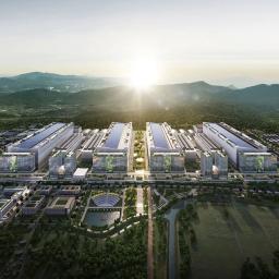
$389.3 billion go to Yongin Semiconductor Cluster to boost DRAM outputSK hynix plans to invest approximately $389.3 billion in the Yongin Semiconductor Cluster, which is the company's largest investment commitment ever and which will make the campus its largest DRAM production site. Meanwhile, Yongin is a greenfield site today.
The first fab in Yongin is expected to commence operations in May 2027, while the remaining fabs will be added sequentially. It takes about a year or 1.5 years or so to fully ramp a DRAM fab, so expect the facility to impact the memory market in 2028 - 2029. Under the company's newly announced plan, construction of all four fabs is now targeted to complete the fourth fab by 2033, instead of the original 2045 timeline. The $389.3 billion investment extends beyond 2033.
$259.5 billion go to Southwestern Semiconductor ClusterUnlike Yongin, the Southwestern Semiconductor Cluster does not even exist. It is currently a planned project, and SK hynix has not even selected a specific site within southwestern Korea. The company says the exact location will be determined after evaluating land availability, electricity, water, transportation, and other infrastructure requirements in consultation with central and local governments.
The cluster is envisioned as SK hynix's next major manufacturing base after Icheon, Cheongju, and Yongin. For now, the planned investment totals approximately $259.5 billion, though given that the project's completion is decades away, we can expect that number to change upwards or downwards depending on the market conditions and the cost of wafer fabrication equipment.
The investment will be phased over many years and cover land acquisition, fab construction, and production tools. SK hynix says preparations must begin now because developing a new semiconductor cluster - including site selection and infrastructure - takes many years. For example, development of the Yongin Cluster took about nine years, according to SK hynix.
Not aloneSK hynix is not alone in investing in South Korea. Samsung on Thursday announced plans to spend some KRW 140 trillion ($90.98 billion) in its operations in South Korea's Chungcheong region.
Under the plan, Samsung Display will expand OLED production in Asan; Samsung Electronics will build five HBM production lines in Onyang and modernize HBM-related facilities in Cheonan; Samsung SDI will establish a battery production line in Cheonan to validate next-generation technologies before deploying them globally; and Samsung Electro-Mechanics will expand AI server package substrate manufacturing in Sejong.