Nvidia Tesla V100: First Volta GPU is one of the largest silicon chips ever
Enlarge (credit: Nvidia)
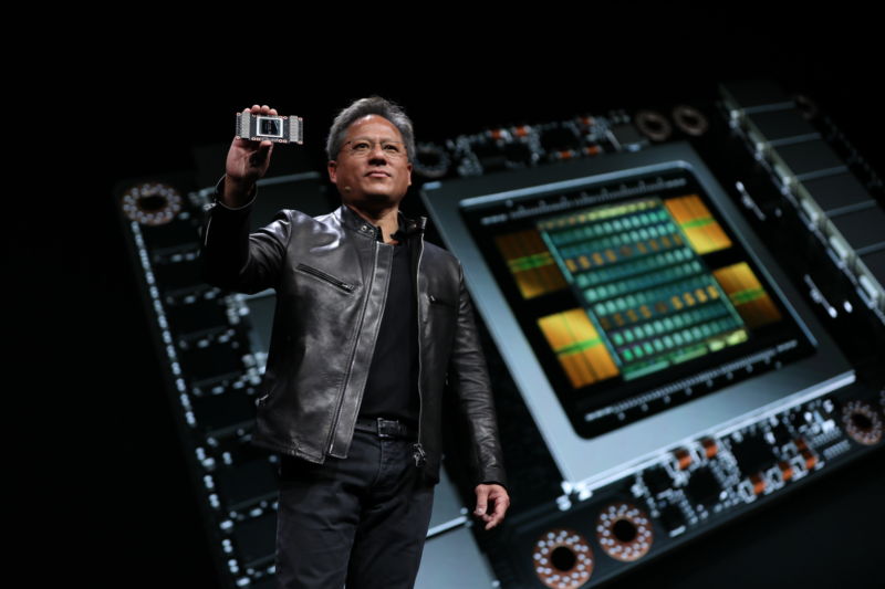
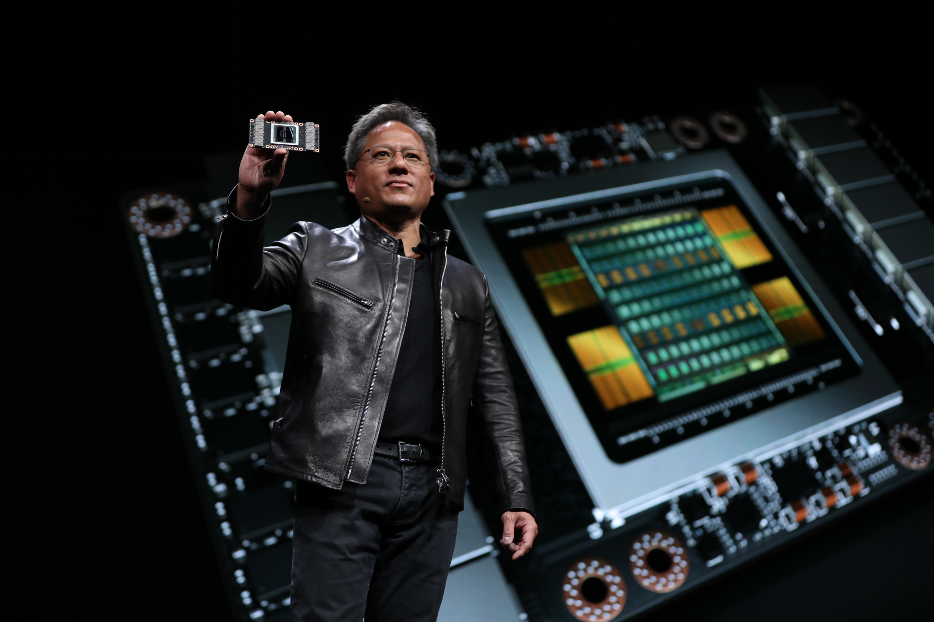
Nvidia has unveiled the Tesla V100, its first GPU based on the new Volta architecture. Like the Pascal-based P100 before it, the V100 is designed for high-performance computing rather than consumer use, but it still provides a tantalising glimpse at what the future might hold for Nvidia's consumer graphics cards.
Volta, which has been on Nvidia's public roadmap since 2013, is based on a dramatically different architecture to Pascal, rather than a simple die shrink. The V100 chip is made on TSMC's 12nm Fin-FET manufacturing process and packs a whopping 21.1 billion transistors on a 815mm^2 die. By contrast, the P100 manages just 15.3 billion transistors on a 610mm^2 die and the latest Titan Xp sports a mere 12 billion transistors on 471 mm^2.
Suffice it to say, V100 is a giant GPU and one of the largest silicon chips ever produced, period.
Read 6 remaining paragraphs | Comments