IBM unveils world’s first 5nm chip
by Sebastian Anthony from Ars Technica - All content on (#2RX9A)
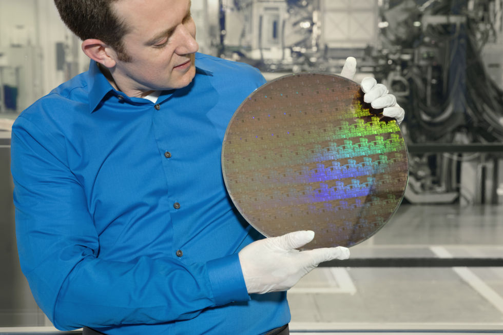
IBM, working with Samsung and GlobalFoundries, has unveiled the world's first 5nm silicon chip. Beyond the usual power, performance, and density improvement from moving to smaller transistors, the 5nm IBM chip is notable for being one of the first to use horizontal gate-all-around (GAA) transistors, and the first real use of extreme ultraviolet (EUV) lithography.
GAAFETs are the next evolution of tri-gate finFETs: finFETs, which are currently used for most 22nm-and-below chip designs, will probably run out of steam at around 7nm; GAAFETs may go all the way down to 3nm, especially when combined with EUV. No one really knows what comes after 3nm.
Read 12 remaining paragraphs | Comments