Intel starts cooking up enhanced 18A-P silicon for would-be foundry customers
by from www.theregister.com - Articles on (#76CBC)
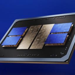 While Intel ramps up production of its 18A process node, the chipmaker has started limited output of its enhanced variant, 18A-P, promising 9 percent higher performance at the same power. At the IEEE's 2026 VLSI Symposium in Hawaii, Intel disclosed that it has started risk production using 18A-P, the first of its planned enhancements for the 18A process, and potentially the first to be used for commercial customers of Intel's foundry biz. Risk production refers to initial low-volume output to qualify a new manufacturing node. Chipzilla says reaching this stage means it is meeting timelines it has shared with customers and partners. The x86 giant launched its first chips made with the base 18A process back in January, in the form of the "Panther Lake" Core Ultra Series 3 processors. But it had already detailed plans for updated versions of the manufacturing tech last year, as reported by The Register at the time. Intel claims 18A-P delivers 9 percent better performance than 18A while consuming the same power as 18A silicon, or, alternatively, 18 percent lower power consumption for the same performance. It achieves these performance and power benefits through a mix of transistor, interconnect, and design technology co-optimizations, the firm says. But a key factor is that 18A-P is said to be fully design rule compatible with 18A, meaning that any chips designed for 18A should be easily transferable for production with Intel's newer process. Industry talk is that Intel's first foundry customers may therefore skip straight to 18A-P. Previously, the chipmaker planned to offer the upcoming and more advanced 14A node as its first mainstream commercial offering but it is understood that chief exec Lip-Bu Tan changed that plan. Intel is also reportedly in talks with Apple to manufacture some of its silicon on 18A or 18A-P. "Our updates and presentations at VLSI signal to Intel Foundry customers and partners that we are fully committed to leading edge process innovation over the long term," said Intel Foundry EVP Naga Chandrasekaran. The other process node variant Intel is working on is called 18A-PT, which is optimized for designs requiring through-silicon vias (TSVs). This is to allow a final product to be assembled by stacking multiple chips or chiplets on top of one another. Industry watchers believe Intel expects AI accelerator designers will favor 18A-PT, as it allows memory tiles to be manufactured separately and integrated during packaging. Also at the VLSI event, Intel disclosed several technologies still under development. These include CFET (Complementary FET) using vertically stacked NMOS and PMOS devices for increased transistor density, and integration of gallium nitride power devices with silicon logic, enabling digital control circuitry alongside high-power transistors in a single process. Speaking at a conference earlier this month, Intel chief financial officer David Zinsner admitted that the firm had bitten off more than it could chew with 18A, referring to the delays in getting it into production last year. "I would say it this way, I don't know, early last year, I think the challenge around 18A was two things. One, we tried to do too much at once. And it took a while to get that settled. And I think second is, we were trying to play performance and yield and trying to improve both at the same time. It was like trying to fly the plane and fix the wing at the same time, basically," he said. (R)