IBM stacks up a sub-nanometer chip future
by from www.theregister.com - Articles on (#76J2Q)
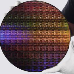 IBM has developed a sub-nanometer (nm) chip technology it says could be used to produce commercial chips within five years, and has mapped a path to 0.1 nm. Big Blue claims its new process node can cram nearly 100 billion transistors onto a silicon die the size of a fingernail, almost double the density of the 2 nm technology it unveiled back in 2021. The new process as disclosed is actually for 0.7 nm or 7 Angstroms (7A), compared with the cutting-edge manufacturing nodes now being prepared for production in 2028 by the likes of Intel and TSMC which are 1.4nm, or 14 Angstroms. Several structural and material innovations have gone into this latest manufacturing method, including a three-dimensional nanostack architecture that sees transistors stacked, with n-type and p-type field-effect transistors (FETs) arranged so that one is layered above the other. "We're announcing it's not just an incremental step, it's a meaningful leap forward, enabling up to 50 percent higher performance, or 70 percent greater efficiency [than 2nm], and pointing to a future where computing becomes significantly more powerful without a corresponding increase in energy," claimed director of IBM Research and IBM Fellow Jay Gambetta. And the firm sees a clear path to shrinking down to one-tenth of a nanometer over the next ten years, he added. "Nanostack is not one innovation. It is actually a device platform that can enable the future of scaling for another decade beyond nanosheet, as you can see from our technology roadmap all the way to 1 Angstrom." Although the firm touts nanostack as the industry's first three-dimensional, nanosheet-based design, Intel was talking about 3D stacking of transistors back in 2023 - though has not so far implemented it. Huawei has also come up with a similar concept in its LogicFolding architecture, using two separate wafers fused together. IBM's nanostack design also has a twist - the transistors in the upper layer are staggered, or offset, from those below. "Nanostack is nanosheet transistors stacking on top of each other. But it's not through a simple monolithic lithography and etch process," said Huiming Bu, VP of Silicon Technology Research & Development at IBM. "What happens here is we actually stack in vertical direction but also stagger, so the front side of each transistor and the backside of each transistor can be contacted independently for signal and power," he added. "Second, the stacking of this transistor is done by single dielectric bonding, which is a key innovation that we have developed. Through that technology, the channel materials, essentially the top FET and the bottom FET, can be optimized independently." IBM says the architecture could support multiple applications such as CPUs, GPUs, mobile chips and memory, such as SRAM. Gambetta hinted that the technology could be used in future AI accelerators. "This is why we were excited by the initial experiment that shows a 40 percent scaling in SRAM. There are many examples of AI chips that are using more SRAM to scale, but fundamentally, it comes down to: can we make transistors more efficient, less power, put more in there?" he said. But IBM no longer manufactures chips itself. When asked which foundry might adopt its sub-nanometer process, Huiming said the nanosheet architecture IBM invented is now used by all leading foundries at this point. "I'm not going to talk about a business model, but it's being adopted by all leading foundries. But today, we are focusing on helping Rapidus to be successful in bringing up 2 nm manufacturing capability in Japan," he stated. Rapidus is a government-backed semiconductor foundry set up to revitalize the nation's semiconductor industry. The nanostack transistor architecture is discussed in a paper, available for download from the IEEE. (R)