Micron announces new 3D NAND process—denser, faster, less expensive

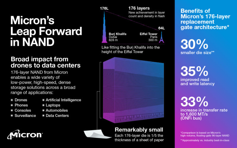
Enlarge / We're all intimately familiar with the Burj Khalifa's relationship to the Eiffel Tower, right? (credit: Micron)
On Monday, memory and storage vendor Micron announced that its new 176-layer 3D NAND (the storage medium underlying most SSDs) process is in production and has begun shipping to customers. The new technology should offer higher storage densities and write endurance, better performance, and lower costs.
Replacement-gate architecture
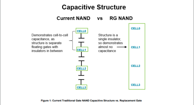
Replacement-gate architecture eliminates gaps between cells and the unintentional capacitive effect those gaps necessarily cause. (credit: Micron)
The new NAND process is Micron's fifth generation of NAND and its second generation of replacement-gate architecture-a replacement to the earlier, floating-gate architecture used by both Micron and Intel in the past. In traditional floating gates, insulators separate individual cells, which results in undesired capacitance between cells.
Micron's replacement-gate architecture instead builds multiple cells into a single insulating structure, virtually eliminating cell-to-cell capacitance, and (according to Micron) increasing write endurance, power efficiency, and performance. The company has not yet provided concrete benchmarks quantifying these claims.
Read 8 remaining paragraphs | Comments