The Post-Silicon future
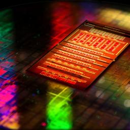
 It's hard to understate the impact of the silicon chip and the advances wrought by Moore's law and steady research and development in miniaturizing transistors on silicon. But we're getting close to the limits, and getting beyond 9nm puts us at the limits of physics, it would seem. So what's next?
IBM is hoping it will be the first to find out. Not one to shy away from the big bets, IBM is putting $3B into researching the next step, including having a go at 7nm processes, new semiconducting materials like Gallium-Arsenide, and technologies like carbon nanotubes and graphene. At 7nm, the game changes significantly, and quantum physics begins to matter as much as traditional physics. Steve Torbak points out there's hope for technologies like racetrack memory and neuromorphic memory, too.
Or maybe, there's still room for improvement with what we've got. We're not done with Systems-on-a-Chip, after all, and DARPA has recently taken this approach to put an entire communications stack on a dime-sized chip.
[Ed. note: All I know is, to watch the next generation of silly cat videos, we're going to need a serious boost in hardware. /grin]
So, if you want a preview of what CPU process nodes will be like in a few years, simply look at what NAND flash is doing today.